2. 电子科技大学光电信息学院 成都 610054
2. School of Opto-Electronic Information, University of Electronic Science and Technology of China Chengdu 610054
In the past years,a doped MgO layer[3, 4, 5],a double protective layer[6, 7, 8],and new materials instead of MgO protective layer[9, 10],have been emerged in many papers,mainly in order to improve the luminous efficiency and reduce power consumption. According to the discharge mechanism of AC PDP,priming electrons are required to ignite a discharge. Recently,our group has studied the application of hexaboride lanthanum (LaB6) in AC PDP. Because of the low work function of LaB6,it was easy to generate priming electrons,and lower firing voltage and shorter discharge delay time were obtained accordingly[11, 12].
In this work,carbon nanotubes (CNTs) were coated on a conventional MgO protective film by a spray coating method as a functional layer. CNT is an excellent field emission material and it has attracted considerable attention due to its excellent electronic and structural properties. Among the various applications,Report on the extraordinary high electron-induced SEE yields for MgO/CNTs suggested the possibility of its application in AC PDP,in which MgO film was deposited on CNTs surface[13]. In this work,we studied the possible application of the CNTs/MgO protective layer to AC PDP by fabricating a prototype of AC PDP and testing the discharge characteristics. This structure is different from that in Ref. [13] which CNTs was coated on MgO protective film to act as a functional layer.
1 ExperimentsIn our experiment,the substrates were provided by Changhong Display Device Co. Ltd.,Mianyang China,which included indium thin oxide (ITO) layer,transparent dielectric layer,and an MgO protective layer. The preparation process of spray coated CNTs was as follows. First,the MWNTs (0.1 g),ethyl cellulose (80 mL),and acetone (120 mL) were mixed and ultrasonic vibrated for 24 h to form a type of solution. Next,the solution was coated on the substrate by a spray gun and dried at 120 ℃ in air for 10 min. To observe the visible light transmittance and discharge properties of fabricated CNTs/MgO protective layer,the products were characterized and analyzed by an ultraviolet-visible spectrophotometer and an AC PDP discharge test system,respectively.
Fig. 1 shows the structure of the AC PDP test cell used in this experiment. Dielectric layers with the thickness of 21μm and barrier ribs with the height of 120 μm were prepared by the screen-printing method. The transparent indium tin oxide (ITO) layer with the thickness of 130 nm was fabricated by the magnetron sputtering method and patterned by the lithography process. The MgO protective layer with the thickness of 800 nm was formed on the dielectric layer by electron beam evaporation and then a very small amount of CNTs was coated on the MgO film as a functional layer. The coplanar gap between the common electrode and the scan electrode was 80 μm,and the width of the barrier was 50 μm. The discharge gas consisted of Ne and Xe at 20~100 torr.
 |
| Fig. 1 Schematic diagram of the AC PDP prototype used in this experiment. |
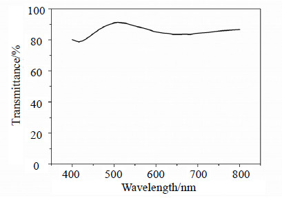
Fig. 2 shows the visible light transmittance of CNTs/MgO protective layer,using a conventional MgO protective layer as a reference. It indicates that,the relative transmittance of CNTs/MgO protective layer is more than 80 % in the 400 nm to 800 nm wavelength range. Especially,in the 500 nm to 550 nm wavelength range,the transmittance is high up to 90%.
 |
| Fig. 2 Visible light transmittances of CNTs/MgO protective layer using a conventional MgO protective layer as a reference. |
Fig. 3 compares the firing voltages of the test panels with a CNTs/MgO protective layer and a conventional MgO protective layer in 5 % and 10 % Xe-Ne,respectively. It is found that no matter how high the pressure is,the discharge voltage of the test panel with CNTs/MgO is lower than that with a conventional MgO layer. Especially,with 100 torr 10% Xe-Ne applied to the testing system,the firing voltage of the AC PDP test cell with CNTs/MgO protective layer is 263.5 V,which is 15 % lower than that with a conventional MgO protective layer (308.5 V). According to Paschen’s law,the firing voltage (Vf) is dependent on the content of gas mixture,the gas pressure,and the emission characteristics of the protective layer. It is defined by the following equation.
| $ {V_f} = \frac{{A(Pd)}}{{\ln \left[ {B\left( {Pd} \right)/\ln \left( {1 + 1/\gamma } \right)} \right]}} $ | (1) |
 |
| Fig. 3 Firing voltages of AC PDP test cells with a CNTs/MgO protective layer and a conventional MgO protective layer versus gas pressure. |
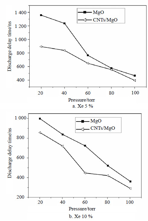
Fig. 4 shows the discharge delay time of the test panels with a CNTs/MgO protective layer and a conventional MgO protective layer,respectively. It is found that the test cell with a CNTs/MgO protective layer always presents much shorter discharge delay time than that with a pure MgO protective layer. The reciprocal of the statistical delay is expressed as ${t_s} = 1/({Y_e}{P_0})$,where ${Y_e}$is the generation rate of priming electrons and ${P_0}$is the probability of a discharge being caused by one initial priming electron[14]. Because ${P_0}$ is constant for a particular cell structure and electric field, ts is determined by the priming electron emission rate. We can assume that the priming electrons are emitted by the field emission of CNTs when the measuring voltages are applied. Before the measuring voltage is applied,CNTs near the anode have a negative charge wall charge induced by the previous discharges because the CNTs are in contact with the insulator. When the measuring voltage is applied,the CNTs act as cathodes,resulting in field electron emission. Then, ts of CNTs/MgO protective layer is reduced. As shown in Fig. 4b,with 100 torr 10% Xe-Ne pressure,the discharge delay time for the PDP cell with a CNTs/MgO protective layer reaches 270 ns,which is 26 % lower than a conventional MgO protective layer (365 ns).
 |
| Fig. 4 Discharge delay time of AC PDP test cells with a CNTs/MgO protective layer and a conventional MgO protective layer versus gas pressure. |
In conclusion,the transmittance and discharge properties of a CNTs/MgO protective layer used in AC PDP have been investigated. Both the firing voltages and discharge delay time of the test cell decrease are attributed to the addition of CNTs functional layer. The electron emission from CNTs can be explained by the field emission,which is different from the mechanism of electron emission from the MgO film and is beneficial to improve the discharge properties of AC PDP.
| [1] | CHEN Y X, LI Q, HU K, et al. Wall-voltage stability in AC-PDP dielectric barrier discharges[J]. IEEE Transactions on Plasma Science, 2013, 41(1): 159-164. |
| [2] | KIM D M, SHIN B J, TAE H S, et al. Improvement of luminous efficacy using short sustain pulse width and long off-time between sustain pulses in AC plasma display panel[J]. IEEE Transactions on Plasma Science, 2013, 41(4): 887-890. |
| [3] | AHNS Il, LEE S E, RYU S H, et al. A study on the secondary electron emission from Na-ion-doped MgO films in relation to the discharge characteristics of plasma display panels[J]. Thin Solid Films, 2009, 517: 1706-1709. |
| [4] | KIM J K. Modification of a driving waveform in an AC plasma display panel with Sc-doped MgO protecting layer[J]. IEEE Transactions on Electron Devices, 2013, 60(8): 2556-2560. |
| [5] | KIM W H, CHO K H, CHOI K C, et al. Influence of gold nanoparticles on the characteristics of plasma display panels[J]. IEEE Transactions on Electron Devices, 2010, 57(10): 2644-2650. |
| [6] | LEE T H, CHEONG H W, KWON O, et al. Application of MgCaO cathode layer to plasma display panel for high luminous efficacy[J]. IEEE Transactions on Electron Devices, 2013, 60(1): 301-304. |
| [7] | PARK C S, TAE H S, JUNG E Y. Influence of Al2O3 reflective layer under phosphor layer on luminance and luminous efficiency characteristics in alternating-current plasma display panel[J]. Thin Solid Films, 2013, 547: 43-46. |
| [8] | JUNG H Y, LEE T H, KWON O, et al. Realization of high luminous efficacy at low voltages in the plasma display panel with SrO-MgO double layer[J]. IEEE Electron Device letters, 2010, 31(7): 686-688. |
| [9] | YASUSHI M, HIDEOMI M, HIROSHI M. A study of the secondary electron yield γ of insulator cathodes for plasma display panels[J]. IEEE Transactions on Electron Devices, 2001, 48(8): 1568-1574. |
| [10] | MOTOYAMA Y, MURAKAMI Y, SEKI M, et al. SrCaO protective layer for high-efficiency PDPs[J]. IEEE Transactions on Electron Devices, 2007, 54(6): 1308-1313. |
| [11] | DENG J, ZENG B Q, WANG X J, et al. Improvement of discharge properties by printing LaB6 films on MgO protective layers in plasma display panel[J]. IEEE Electron Device Letter, 2013, 34(8): 1026-1028. |
| [12] | WANG X J, DENG J, LIU Z Y, et al. Discharge characteristics of LaB6 protecting thin films in ac plasma display panel[J]. Chinese Science Bulletin, 2012, 57: 2544-2546. |
| [13] | LEE W T, IM S J, HAN J G, et al. MgO/carbon nanotubes protective layer in ac-plasma display panels[J]. Japanese Journal of Applied Physics, 2002, 41: 6550-6552. |
| [14] | OKADA T, YOSHIOKA T. Application of carbon nanotubes as a source of priming electrons in ac plasma display panels[J]. Applied Physics Letter, 2008, 93: 171501. |
 2016, Vol. 45
