ISSN
ISSN 


 下载:
下载:

-
Hydrogenated amorphous silicon (a-Si: H) films have a wide range of practical applications, particularly in mirco-electromechanical system (MEMS), photovoltaic and photodetection. And plasma enhanced chemical vapor deposition (PECVD) is generally used as the deposition method of a-Si: H films for enabling large area deposition and high-quality film. Previous studies have demonstrated the fact of surface morphology of the PECVD-deposited a-Si film related to the substrate material[1-6]. Ref. [1] reported that smooth a-Si film without hillocks is formed on the 100 nm oxide/Si substrate while a rough surface with many hillocks is formed on the crystalline Si substrate. Ref. [2] discussed the influence of the PECVD parameters on the surface roughness of a-Si: H film, and the optimized deposition conditions to suppress the formation of gas bubbles in thick a-Si: H film deposited on silicon substrate. Ref. [3] considered some strategies to mitigate the formation of those micro-bubbles, and found a dramatic improvement in surface roughness quality in their experiment. In addition, some works have demonstrated that bubble defects are also formed on a-Si film after the process of annealing, which is resulted from the accumulation of hydrogen molecules on the film-substrate interface as hydrogen diffused from the film[4-6]. Previous works on the surface morphology of the PECVD-deposited a-Si film mainly focused on the bubble defects’ formation mechanism and the corresponding suppression methods, but ignored the potential applications of this kind of self-formed surface microstructure.
In this paper, we prepared a-Si: H film on crystalline silicon substrate, with nonuniformly distributed bubbles observed on the surface, which is consistent with the results in previous literatures. The latest advance in micro- and nano-fabrication lies in self-assembly or self-organization techniques[7-9], but to the best of our knowledge, few reports on this kind of novel self-formed technique. This technique has advantages in easier process and lower cost, indicates a high feasibility and a good prospect in the field of nanophotonics and MEMS.
-
The a-Si: H film was deposited directly on crystalline silicon substrate by PECVD with RF power of 80 W, chamber pressure of 370 mTorr, temperature of 320 ℃ and SiH4 gas flow rate of 100 sccm. Then, without breaking vacuum, the SiNx film was also prepared by PECVD with RF power of 140 W, chamber pressure of 480 mTorr, temperature of 320 ℃ and NH3/SiH4 gas flow rate of 225/50 sccm. The surface morphology and bubble defect microstructure are characterized by using optical microscope and scanning electron microscope (SEM).
-
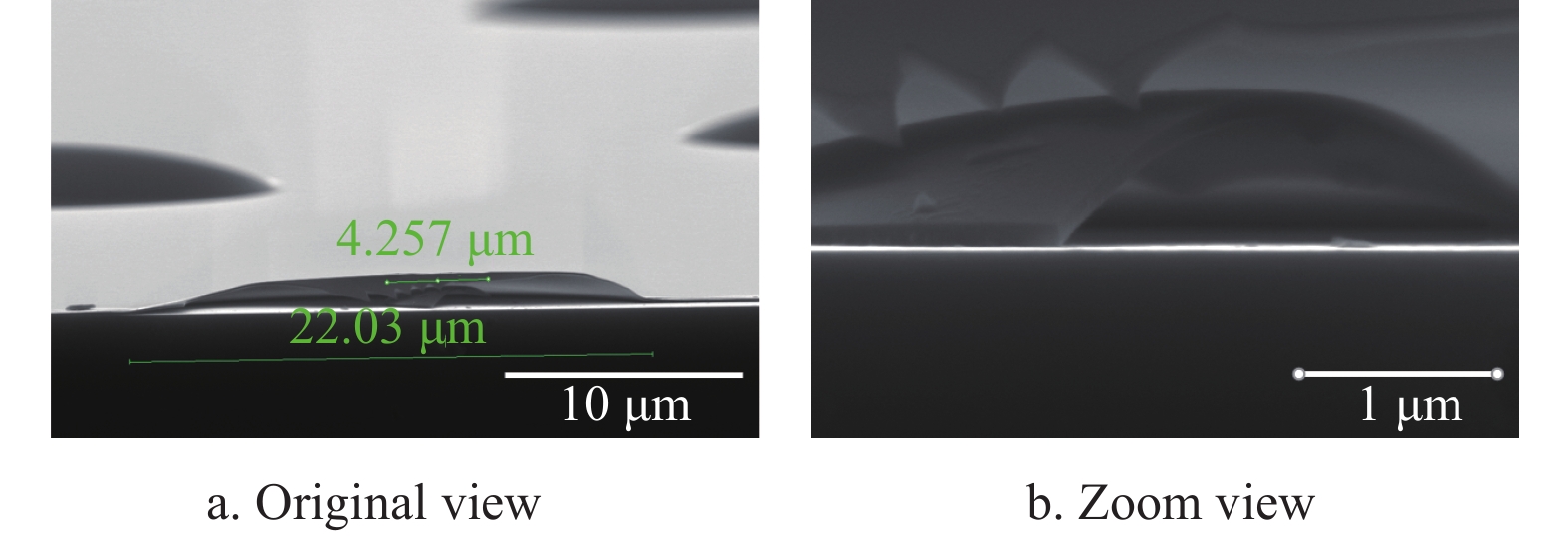
Nonuniformly distributed micro-bubbles are observed on the surface of the deposited a-Si on crystalline silicon substrate. Fig. 1 shows representative micro-bubbles obtained by optical microscope, and the characteristics size of micro-bubbles decreases with the deposition time, and the density increases with the deposition time. The formation of such bubble defects in a-Si: H films has been previously reported and has been attributed to trapped hydrogen gas unable to escape[3-6]. The perfect dome morphology is as a result of film stress. The film stress increases with the deposition time, which leads to a smaller size of micro-bubbles, which is consistent with the results obtained in the experiment.
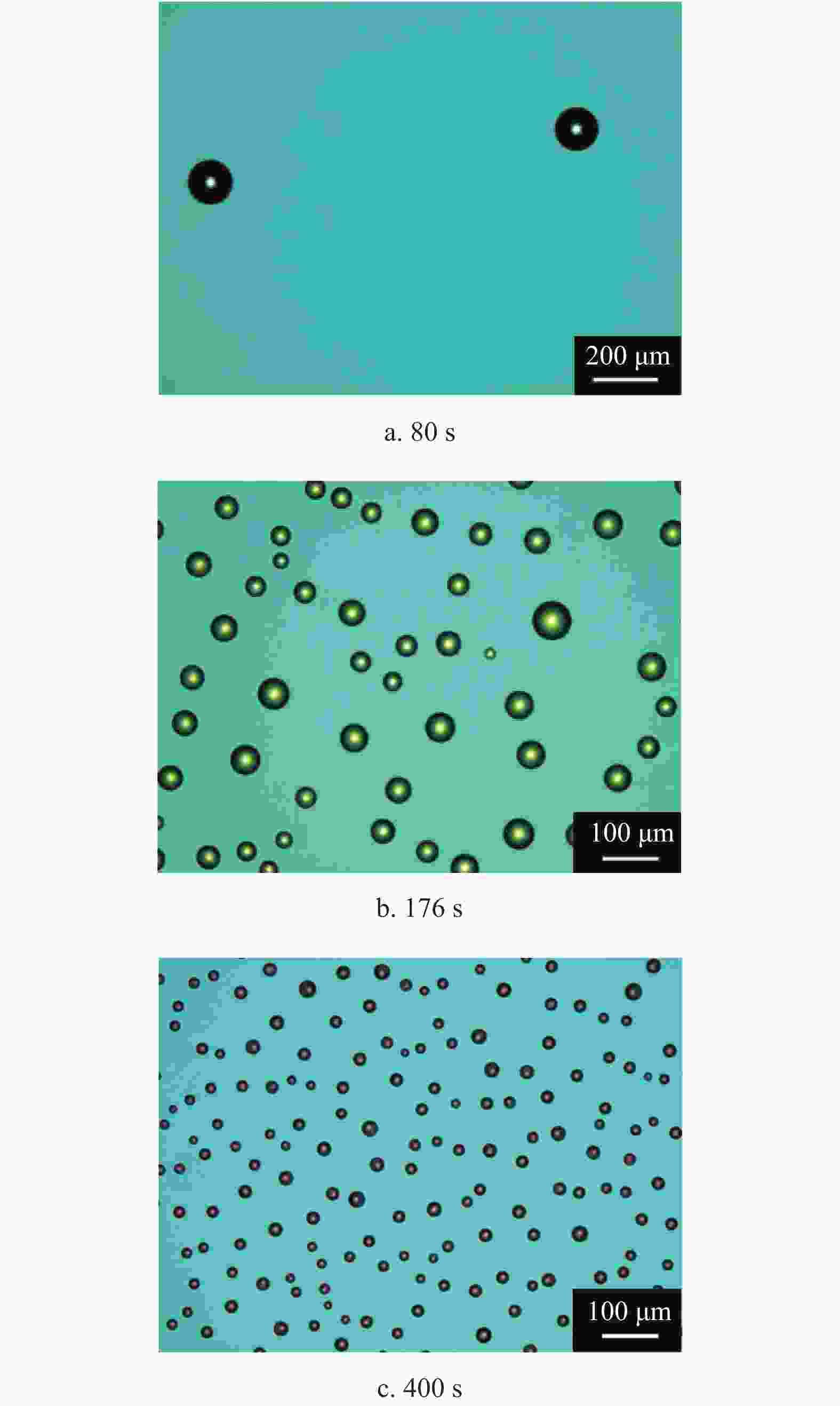
Figure 1. Optical micrograph of single layer a-Si film with nonuniform bubbles formation at varied deposition times
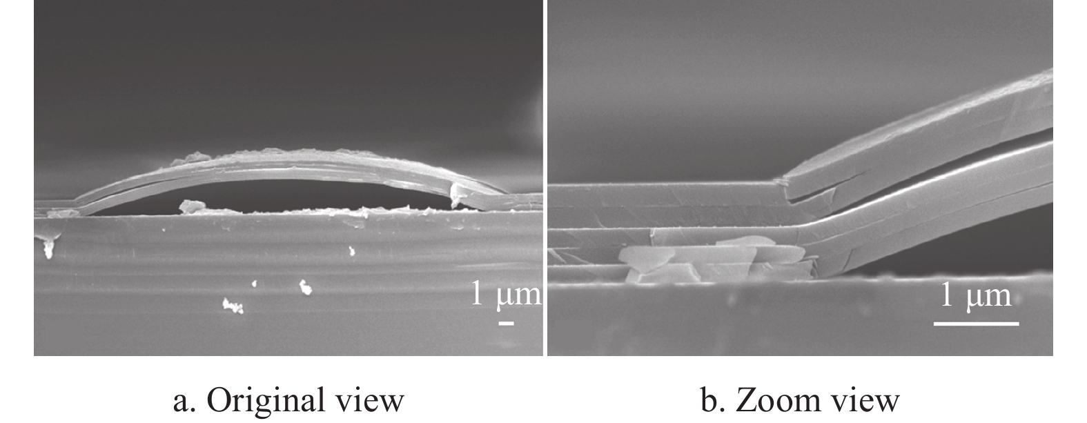
As shown in Fig. 2, the cross-section SEM image of as-prepared a-Si film demonstrated an interesting microstructure characteristic with a double-dome morphology, as shown in Fig. 2a. Fig. 2b depicted that the inner dome presented an appearance of discontinuous film, while the outer dome presented an appearance of continuous film. The double-dome morphology is not universal, most of the micro-bubbles have single-dome morphology, as shown in Fig. 3~Fig. 5. The deposition of a-Si films is more complicated than simple homoepitaxy. Growth mechanisms are related to varying sticking coefficients, extraction reactions, precursor diffusion, hydrogen diffusion and evolution, and subsurface cross linking of silicon[10]. Here the smaller bubble formed as inner dome is attributed to low cluster mobility at the nucleation sites. This double-dome morphology effect might be suppressed by optimized fabrication process.
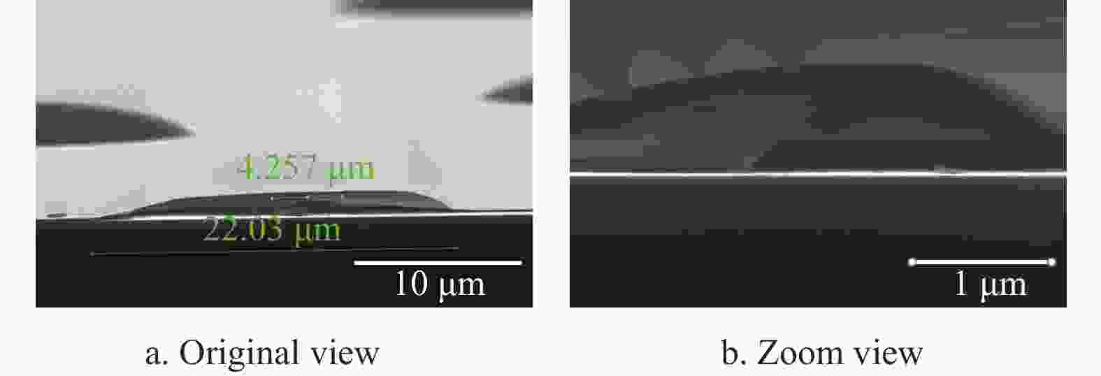
Figure 2. Cross-section SEM image of as-prepared a-Si film with dual-bubbles formation
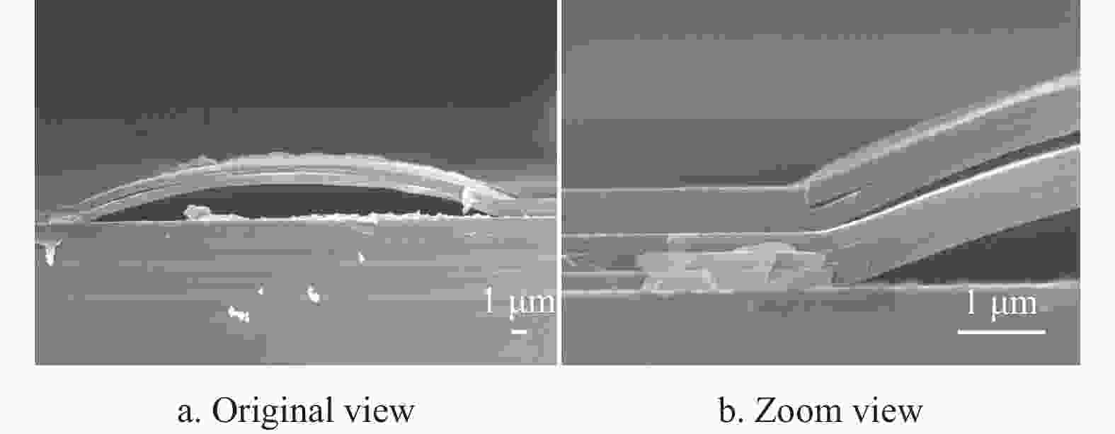
Figure 3. Cross-section SEM image of SiNx/a-Si alternative layer with 2-pairs prepared by PECVD
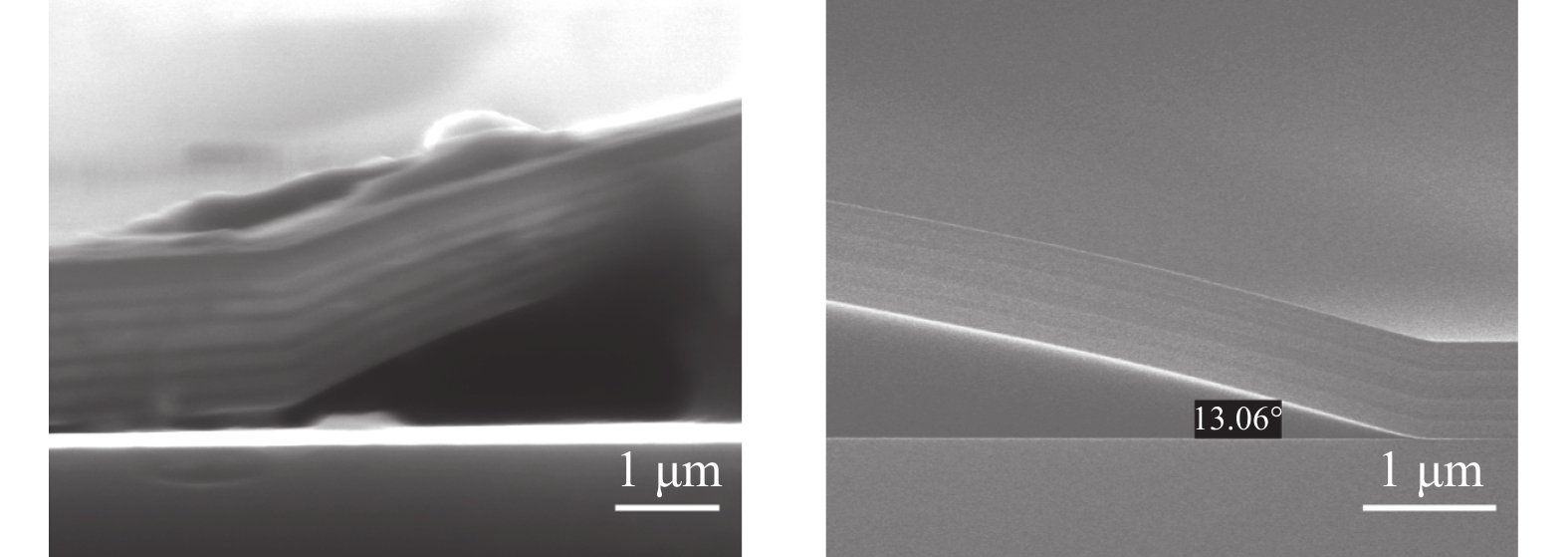
Fig. 3 shows the micrography of SiNx/a-Si alternative layer with 2-pairs prepared on the as-prepared a-Si film with self-formed surface microstructures. The top and bottom layers are both a-Si films. As shown in Fig. 3b, the subsequent SiNx/a-Si film deposition on as-prepared a-Si film shows perfect conformal characteristics. However, the delamination occurred between the third layer and the fourth layer (from bottom to top), which is attributed to the film stress and film adhesion. Further optimization of fabrication process can suppress the delaminated phenomenon.
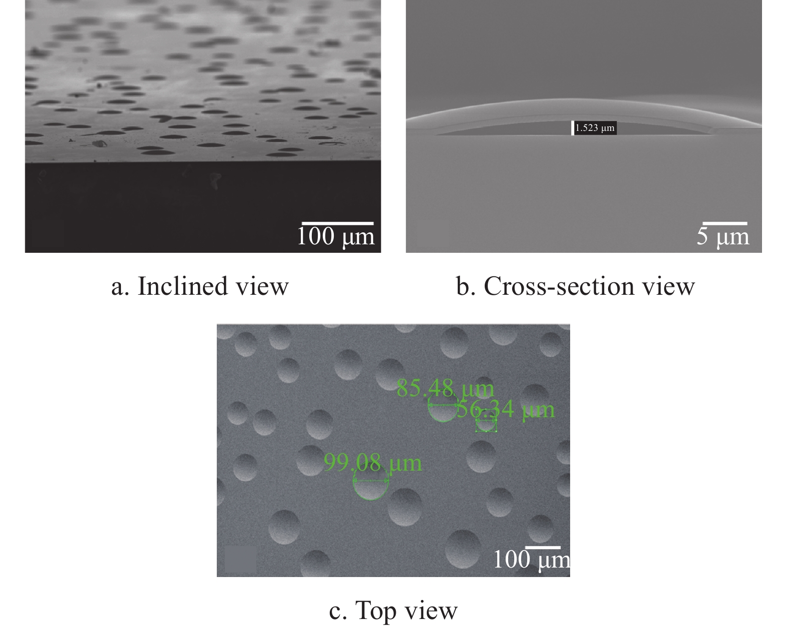
To verify the strong mechanical properties of our self-formed silicon microstructures, we further prepared SiNx/a-Si alternative layer with 4-pairs on as-prepared a-Si film. The morphology characteristics are shown in Fig. 4 and Fig. 5, we can see that the dome-shaped multi-shell microstructures show perfect conformal characters with no distinct structural collapse, which demonstrated a certain mechanical strength. The total thickness of SiNx/a-Si alternative layer is approximately 0.74 μm with an improved film adhesion and uniformity. Such a dome-shaped multi-shell microstructure may have lots of potential applications in the field of nanophotonics and MEMS.
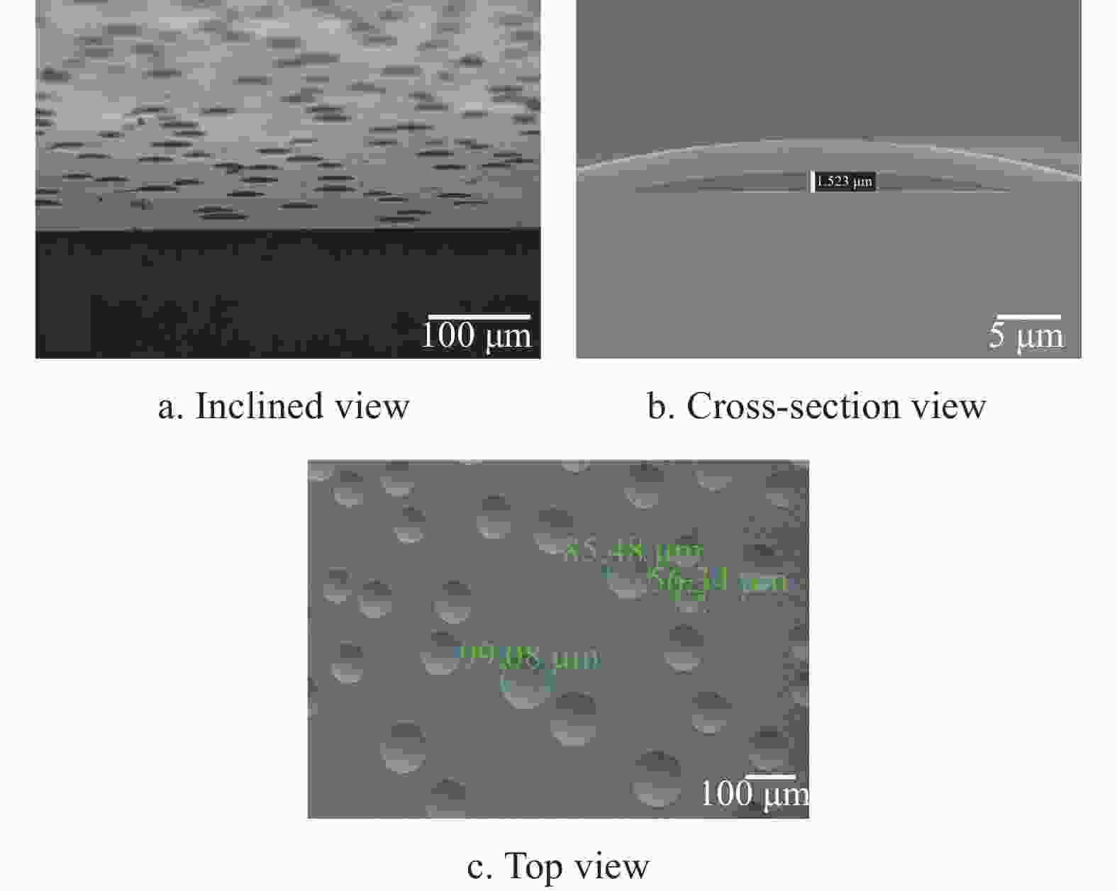
Figure 4. SEM image of SiNx/a-Si alternative layer with 4-pairs prepared by PECVD
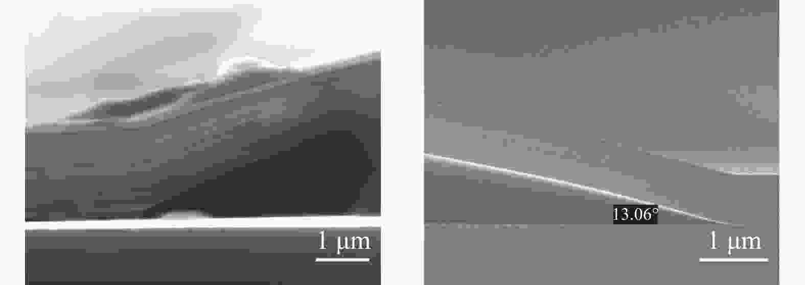
Figure 5. Cross-section SEM image of SiNx/a-Si alternative layer with 4-pairs prepared by PECVD at different self-formed bubbles sites
-
We can conclude three unique characteristics of the dome-shaped multi-shell microstructure: 1) a self-formed microstructure with a dome-shape; 2) controllable size of structure; 3) good mechanical properties. Based on these three characteristics, we propose and discuss three potential applications here.
-
Considering the characteristics of self-formed curved surface, the surface plasmons in graphene can be trapped and guided in its curved landscapes. Ref. [11] demonstrated that graphene placed on top of curved substrates offers a novel approach for trapping and guiding surface plasmons. Monolayer graphene with a spatially varying curvature exhibits an effective trapping potential for graphene plasmons near curved areas. This concept can be utilized in other 2D materials for their plasmons excited. Furthermore, some studies have demonstrated the multiple optical resonance properties involved in dome-shaped micro/nanostructures, including localized surface plasmon resonance (LSPR) modes, waveguide modes, whispering gallery modes (WGMs). A similar work reported by Ref. [12] has demonstrated the feasibility of using dome-shaped resonators based on the whispering gallery modes as an untethered sensing element for remote temperature measurement.
-
We considered the perfect self-formed dome-shape microstructures and their good mechanical properties, which provide new possibilities for the fabrication of three-dimensional microstructure as well as some novel sensors. Some arched or domed MEMS microstructure can be fabricated, as shown in Fig. 6. By depositing or transferring two materials with different thermal expansion coefficients on the as-prepared a-Si film to form a bi-material cantilever beam, the underneath a-Si film can be removed by wet-etching, and the top films can be retained as the basic components of a mechanical actuated sensor, which can be designed for thermal sensing, stress sensing. Similar works have been reported by Ref. [13-14]. They present a plasmonic metamaterial that supports the thermomechanically coupled optical and mechanical resonances for controlling optical damping of mechanical resonance. However, the systems driven by metamaterial-based configuration are much more complicated, and a multi-step lithography process is required. Our self-formed dome-shape microstructure provide a easier fabrication of cantilever structures.

Figure 6. Schematic of mechanical actuated sensors
-
The good mechanical properties of the dome-shaped microstructures provide the possibility for micro-lens design and fabrication. Single micro-lens and micro-lens arrays have been developed in the past for applications in photolithography, imaging, and light communications. And the common fabrication methods include soft lithographic techniques or femtosecond laser direct writing[15-16], which is costed and even complicated. This work provided a novel method for the optimized fabrication of the micro-lens. It should be noted that the random distribution of the bubbles in our self-formed fabrication method makes it difficult to fabricate the array patterns. Accordingly, it requires further studies on the bubbles’ distribution mechanism and control means for enabling the potential application in micro-lens array.
-
We demonstrated that the nonuniformly distributed bubble defects are formed during the process of a-Si: H films deposited on crystalline silicon substrate. And dome-shaped multi-shell microstructures are formed by SiNx/a-Si alternative layers deposited on the as-prepared a-Si: H films with good adhesion between film layers and no distinct structural collapse, whose size can be controlled by fabrication process. These self-formed dome-shaped microstructures have potential applications in nanophotonics and optical sensing fields. This work also provides some processing ideas for complex 3D microstructures and MEMS sensors design.
A Self-Formed Silicon Surface Microstructure: Surface Characterization and Potential Applications
-
摘要: 采用等离子体增强化学气相沉积法(Plasma Enhanced Chemical Vapor Deposition, PECVD)制备掺氢非晶硅膜,并对其表面结构学进行研究。该文发现在晶体硅衬底上沉积非晶硅薄膜时,会在表面形成非均匀分布的起泡缺陷。在已制备的非晶硅薄膜上进一步沉积了氮化硅/非晶硅的交替层,在起泡缺陷原位形成了一个完美的穹顶多壳的微结构,并且没有明显的结构坍塌。该文总结了自成形穹顶微结构的3个独特的结构特性,并进一步指出了该自成形穹顶微结构在纳米光学和微机电系统中的潜在应用。Abstract: The morphology of hydrogenated amorphous silicon (a-Si: H) films grown by plasma enhanced chemical vapor deposition (PECVD) is studied. Nonuniformly distributed bubble defects are formed during the process of a-Si: H films deposited on crystalline silicon substrate. The SiNx/a-Si alternative layers are deposited on the as-prepared a-Si: H film, a perfect dome-shaped multi-shell microstructure was formed at the site of the blister defect, and no distinct structural collapse was observed. Three unique characters of the self-formed dome-shape microstructure are concluded, and the potential applications of the proposed self-formed dome-shape microstructure in nanophotonics and MEMS are also pointed out.
-
Key words:
- MEMS /
- amorphous silicon films /
- blister defect /
- self-formed /
- silicon micro/nanostructures
-
Figure 1. Optical micrograph of single layer a-Si film with nonuniform bubbles formation at varied deposition times
Figure 2. Cross-section SEM image of as-prepared a-Si film with dual-bubbles formation
Figure 3. Cross-section SEM image of SiNx/a-Si alternative layer with 2-pairs prepared by PECVD
Figure 5. Cross-section SEM image of SiNx/a-Si alternative layer with 4-pairs prepared by PECVD at different self-formed bubbles sites
-
[1] CHUNG C K, TSAI M Q, TSAI P H, et al. Fabrication and characterization of amorphous Si films by PECVD for MEMS[J]. Journal of Micromechanics and Microengineering, 2004, 15(1): 136-142. [2] YAN X, FENG F, ZHANG J, et al. Smooth surface morphology of hydrogenated amorphous silicon film prepared by plasma enhanced chemical vapor deposition[J]. Plasma Science and Technology, 2009, 11(5): 569-575. doi: 10.1088/1009-0630/11/5/11 [3] RATNAYAKE D, MARTIN M D, GOWRISHETTY U R, et al. Engineering stress in thin films for the field of bistable MEMS[J]. Journal of Micromechanics and Microengineering, 2015, 25: 125025. doi: 10.1088/0960-1317/25/12/125025 [4] WANG J L, WU L X, CHEN X, et al. Avoiding blister defects in low-stress hydrogenated amorphous silicon films for MEMS sensors[J]. Sensors and Actuators A: Physical, 2018, 276: 11-16. doi: 10.1016/j.sna.2018.04.021 [5] MISHIMA Y, YAGISHITA T. Investigation of the bubble formation mechanism in a-Si: H films by Fourier-transform infrared microspectroscopy[J]. Journal of Applied Physics, 1988, 64(8): 3972-3974. doi: 10.1063/1.341355 [6] SHANKS H R, LEY L. Formation of pin holes in hydrogenated amorphous silicon at high temperatures and the yield strength of a-Si: H[J]. Journal of Applied Physics, 1981, 52(2): 811-813. doi: 10.1063/1.328767 [7] FAN J A, WU C H, BAO K, et al. Self-assembled plasmonic nanoparticle clusters[J]. Science, 2010, 328(5982): 1135-1138. doi: 10.1126/science.1187949 [8] FRANKLIN D, HE Z Q, ORTEGA P M, et al. Self-assembled plasmonics for angle-independent structural color displays with actively addressed black states[J]. Proceedings of the National Academy of Sciences, 2020, 117(24): 13350-13358. doi: 10.1073/pnas.2001435117 [9] KLINKOVA A, CHOUEIRI R M, KUMACHEVA E. Self-assembled plasmonic nanostructures[J]. Chemical Society Reviews, 2014, 43(11): 3976-3991. doi: 10.1039/c3cs60341e [10] TANENBAUM D M, LARACUENTE A L, GALLAGHER A. Surface roughening during plasma-enhanced chemical-vapor deposition of hydrogenated amorphous silicon on crystal silicon substrates[J]. Physical Review B, 1997, 56(7): 4243-4250. doi: 10.1103/PhysRevB.56.4243 [11] SMIRNOVA D, MOUSAVI S H, WANG Z, et al. Trapping and guiding surface plasmons in curved graphene landscapes[J]. ACS Photonics, 2016, 3(5): 875-880. doi: 10.1021/acsphotonics.6b00116 [12] IOPPOLO T, MANZO M. Dome-shaped whispering gallery mode laser for remote wall temperature sensing[J]. Applied Optics, 2014, 53(22): 5065-5069. doi: 10.1364/AO.53.005065 [13] ZHU H, YI F, CUBUKCU E. Plasmonic metamaterial absorber for broadband manipulation of mechanical resonances[J]. Nature Photonics, 2016, 10(11): 709-714. doi: 10.1038/nphoton.2016.183 [14] QIAN Z Y, KANG S H, RAJARAM V, et al. Zero-power infrared digitizers based on plasmonically enhanced micromechanical photoswitches[J]. Nature Nanotechnology, 2017, 12(10): 969-973. doi: 10.1038/nnano.2017.147 [15] CHRONIS N, LIU G L, JEONG K H, et al. Tunable liquid-filled microlens array integrated with microfluidic network[J]. Optics Express, 2003, 11(19): 2370-2378. doi: 10.1364/OE.11.002370 [16] CHEN Z H, YUAN H B, WU P C, et al. Variable focus convex microlens array on K9 glass substrate based on femtosecond laser processing and hot embossing lithography[J]. Optics Letter, 2022, 47(1): 22-25. doi: 10.1364/OL.448344 -

 点击查看大图

图(6)
计量
- 文章访问数: 2039
- HTML全文浏览量: 593
- PDF下载量: 79
- 被引次数: 0