ISSN
ISSN 


 下载:
下载:
-
In recent decades, CsI(Tl) scintillators have been widely used as the converter for X-ray imaging detector because of its high scintillation efficiency, proper emission wavelength matching CCD cameras, and its ability to form micro-columnar morphology at vacuum deposition. CsI(Tl) scintillator tends to grow on substrates in such a way that most of the grains in the film develop a texture, that is, most grains are oriented so that the grains are almost perpendicular to the film-substrate interface.
Since reported in 1969, the micro-columnar structure of deposited CsI(Tl) film has been widely studied, such as the influence of deposition conditions vapor pressure, substrate temperature[1-2], deposition rate[3] and annealing process[1-3] on the columnar morphology, and light output and imaging quality of CsI(Tl) films. The patterned substrate[4-5] and coating reflective layer[6] were employed to control the micro columns, and then improve the light output and the spatial resolution of CsI(Tl) scintillation film. Additionally, the CsI(Tl) layer were coupled with amorphous silicon photodiode arrays to detect the charged particles[7]. The crystalline properties of CsI(Tl) films deposited on LiF single crystals with (100) cleavage plane and its dewetting behavior have been studied and found (110) and (112) preferred orientations different to that of CsI powder[8-10].
In this work, CsI(Tl) scintillator films were fabricated by thermal evaporation method on monocrystalline Si and polycrystalline Pt/Si substrates. These films with different thickness were prepared under the same process conditions. The surface morphology of film was observed by FEI-SEM. The films with different thickness showed different crystalline properties according to their X-ray diffraction (XRD) patterns.
-
CsI(Tl) scintillation films were fabricated by the thermal evaporation method from molybdenum boat. Mainly two types of substrates were chosen to test the thickness influence on microstructure: monocrystalline silicon with the (400) cleavage plane as orienting substrate and polycrystalline Pt/Si as non-orienting one. The souse material was the CsI(Tl) blocks whose doping concentration of Tl was 0.1mol%. CsI(Tl) films were fabricated at the same evaporation pressure (at 10-4Pa level) and substrate temperature (at room temperature). And the temperature of Mo boat was set at 450~500 ℃ to make sure a comparatively low deposition rate ( < 2 nm/s) that may ensure high crystal quality. The microstructure of CsI(Tl) film was affected by the layer thickness[11]. Therefore, deposited layers with different thicknesses were prepared on each kind of substrate. The samples with thicknesses of 70 μm and 100 μm deposited on monocrystalline silicon substrate were labeled as samples A and B. Analogously, samples C and D deposited on polycrystalline Pt/Si substrate were 70 μm and 100 μm thicknesses respectively.
The crystal structure of CsI(Tl) films was examined by high resolution X-ray diffraction (Philips PW1710) in CuKα radiation with an analysis range 2θ of 20°~90°. The surface morphology of films was observed by FEI-SEM (QUANTA FEG 450).
-
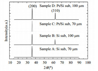
The XRD patterns of sample A and B with different thickness on monocrystalline Si substrate are shown in Fig. 1. Microstructural characteristic of a film is affected by its property and the property of the substrate. The XRD pattern of sample A with 70 μm thickness only shows a strong (200) preferred orientation. That of sample B with 100 μm thickness shows two relatively strong preferred orientations (200) and (310). While, the XRD patterns of sample C and D with different thickness on polycrystalline Pt/Si substrate show similar patterns. The film grows initially as independently nucleated islands which grow into the vapor along the vapor-substrate interface. Thereafter, these islands eventually coalesce to form a continuous film which will subsequently thicken, and the microstructure evolves through a sequence of stages. Polycrystalline films can therefore develop restricted crystallographic orientations during the thickening process of the films[11].

Figure 1. XRD patterns of the CsI(Tl) scintillating films
The only difference between sample A and B (or sample C and D) is the thickness. When the film is relatively thin, the growth of grains is affected strongly by the crystal structure of the substrate, and only (200) plane is preferred. While, the influence decreases as the thickness increases leading to other preferred planes. In this case, the (310) planes is preferred because of its relatively low surface energy. Besides, the grains tend to agglomerate and disorganize as film thickness increases, which lead to polycrystalline structure of the films.
-
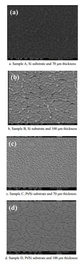
The surface morphology of sample A, B, C and D prepared in the same deposition condition are shown in Fig. 2. The surface morphology of sample A with 70 μm thickness is continuous and compact, and the film surface is smooth. That of sample B with 100 μm thickness is discontinuous covered with voids. Analogously, Sample C with 70 μm thickness shows a continuous and compact surface morphology. Sample D with 100 μm thickness shows a discontinuous surface morphology with cracks. X-ray diffraction is an available method that can be used to infer microstructure of crystalline films. The normal spacing dhkl between adjacent crystallographic planes within a family of planes with indices (hkl) is determined by means of Bragg’s law. According to the XRD patterns of samples and Bragg’s law, the interplanar spacing dhkl of the preferred orientation planes can be calculated. The XRD pattern of sample A with 70 μm thickness shows a strong (200) preferred orientation, whose dhkl is 0.228 5 nm. The intensity of (200) plane is very strong, which indicates most grains grow along the (200) plane and microstructure is good. While that of sample B with 100 μm thickness shows two relatively strong (200) and (310) orientation planes, whose dhkl are 0.228 5 nm and 0.144 6 nm respectively.

Figure 2. Surface morphology of samples prepared at the same condition
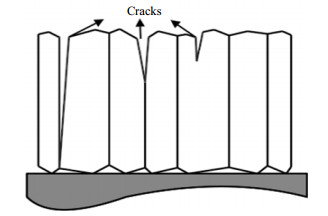
As the lattice density of crystal is constant, the atomic arrangement within the family of crystal planes with bigger interplanar spacing will be denser. The denser atoms reduce the attraction of lattice plane to the extraneous atoms, which slows down the growth rate of grains and laterally spreads the lattice planes with the orientation (200). Conversely, if the interplanar spacing is small, the atomic density of crystal plane will be small, and the attraction to extraneous atoms will increase and the growth rate of grains will be fast, which leads to the lateral spreading of the lattice planes with the orientation (310) diminishing. As the evaporation rate is constant, the atomicity arriving at the substrate surface in unit time is invariable and the grains with the orientation (310) are longer and thinner than the grains with the orientation (200). Meanwhile, different growth rates of lattice plane will produce crystal defects at the grain boundaries, which lead to the distortion and high energy in the boundaries. These behaviors will result in crystal defects within crystal. While the energy is overloaded, the stress will be partially relieved by the process of cracks, as shown in Fig. 3.

Figure 3. Microstructure models of CsI(Tl) films with crack defects
In addition, the substrate produces a stress on grains and this stress will decrease during the thickening of the polycrystalline film, which strongly influences the formation of the grain structure and continued structure evolution such as the orientation (200) and later orientation (310). In the pre-coalescence process, a film forms through heterogeneous nucleation of particles which partially wet the substrate surface. As islands coalesce they can increase in size until they impinge on each other to form a continuous film. If the islands do not have sufficient mobility to align crystallographically at this point, they will join with an intervening grain boundary which is a form of grain growth. Before complete coalescence, the islands are randomly oriented. As deposited at a low temperature (room temperature), the CsI(Tl) films tend to have a non-equiaxed microstructure such as the model shown in Fig. 3. It is likely that deposition is carried out at such a low temperature that the significant grain boundary motion does not occur during coalescence or thickening[12]. Initial crystallographic orientations of the nascent film which minimizes surface and interface energies are favored over others, and the nucleation rates for clusters with lower energy orientations are greater than those for others. This can therefore lead to the development of restricted crystallographic orientations.
-
In this work, CsI(Tl) scintillation films with two different thicknesses were fabricated by the thermal evaporation method on monocrystalline Si and polycrystalline Pt/Si substrates. The films with the thickness 70 μm have an only strong preferred orientation (200) and have a continuous and compact surface morphology. While the films with the thickness 100 μm have two relatively strong preferred orientations (200) and (310) whose surface morphologies are discontinuous and have lots of cracks. Grains were affected by the stress of substrates, and this stress would decrease during the thickening of films, which leads to other preferred orientation. According to the XRD patterns of samples and Bragg’s law, the inter-planar spacing dhkl of the preferred orientation planes (200) and (349) were 0.228 5 nm and 0.144 6 nm respectively. As the lattice density of crystal and the evaporation rate were constant, the growth rate of the grain with the preferred orientation planes (310) was longer and thinner than that of the grain with the preferred orientation planes (200). Moreover, different growth rates of the grains could result in the overloaded energy at the grain boundaries. These phenomena were the main causes of crystal defects within crystal.
-
摘要: 掺铊碘化铯(CsI(Tl))闪烁薄膜因其具有连续致密的微晶柱结构而被广泛应用。该文采用真空热蒸镀方法在单晶硅(Si)衬底和多晶铂硅(Pt/Si)衬底上制备不同厚度的CsI(Tl)薄膜,研究不同衬底上薄膜厚度增加过程中微晶柱结构中出现的裂纹形貌。不同厚度的CsI(Tl)薄膜制备工艺条件相同。通过X射线衍射图谱(XRD)和扫描电子显微照片(SEM)表征CsI(Tl)薄膜的结晶质量和微晶柱结构形貌,研究不同衬底上CsI(Tl)薄膜的微晶柱结构在生长过程中发生的变化。建立CsI(Tl)薄膜的微结构模型研究单晶薄膜中晶面间距对薄膜微晶柱结构的影响。Abstract: Thallium doped cesium iodide (CsI(Tl)) scintillator films are widely used for their dense micro-columnar structure. In this work, CsI(Tl) films with different thickness were fabricated on monocrystalline silicon substrate and polycrystalline Pt/Si substrate by the thermal deposition method. These scintillator films with different thickness were manufactured under the same process conditions and prepared for experiments. The microcrystalline column structures were different during the thickness of films. X-ray diffraction (XRD) and scanning electron microscopy (SEM) were used to investigate the crystal quality and microcrystalline column morphology. The microstructure model of the CsI(Tl) film was built to illustrate the influence of the interplanar spacing on microcrystalline column structures of the monocrystalline film.
-
Key words:
- CsI(Tl) scintillator film /
- interplanar spacing /
- microcrystalline column /
- SEM /
- XRD
-
[1] CHA B K, SHIN J H, BAE J H, et al. Scintillation characteristics and imaging performance of CsI:Tl thin films for X-ray imaging applications[J]. Nuclear Instruments & Methods in Physics Research A, 2009, 604:224-228. http://cn.bing.com/academic/profile?id=2007067570&encoded=0&v=paper_preview&mkt=zh-cn [2] CHA B K, BAE J H, LEE C, et al. The sensitivity and spatial resolution dependence on the microstructures of CsI:Tl scintillation layer for X-ray imaging detectors[J]. Nuclear Instruments & Methods in Physics Research A, 2011, 633:S297-S299. http://cn.bing.com/academic/profile?id=2022668600&encoded=0&v=paper_preview&mkt=zh-cn [3] FUJIEDA I, CHO G, DREWERY J, et al. X-ray and charged particle detection with CsI(Tl) layer coupled to a-Si:H photodiode layers[J]. IEEE Transactions on Nuclear Science, 1991, 38(2):255-262. doi: 10.1109/23.289306 [4] JING T, GOODMAN C A, DREWERY J, et al. Amorphous silicon pixel layers with cesium iodide converters for medical radiography[J]. IEEE Transactions on Nuclear Science, 1994, 41(4):903-909. doi: 10.1109/23.322829 [5] JING T, CHO G, DREWERY J, et al. Enhanced columnar structure in CsI layer by substrate patterning[J]. IEEE Transactions on Nuclear Science, 1992, 39(5):1195-1198. doi: 10.1109/23.173177 [6] NAGARKAR V V, GUPTA T K, MILLER S R, et al. Structured CsI(Tl) scintillators for X-ray imaging applications[J]. IEEE Transactions on Nuclear Science, 1998, 45(3):492-496. doi: 10.1109/23.682433 [7] JING T, GOODMAN C A, DREWERY J, et al. Detection of charged particles and X-rays by scintillator layers coupled to amorphous silicon photodiode arrays[J]. Nuclear Instruments & Methods in Physics Research A, 1996, 368:757-764. http://cn.bing.com/academic/profile?id=2060508258&encoded=0&v=paper_preview&mkt=zh-cn [8] FEDOROV A, LEBEDINSKY A, MATEYCHENKO P. Dewetting behavior of CsI layers on LiF substrate[J]. Journal of Crystal Growth, 2011, 318:595-598. doi: 10.1016/j.jcrysgro.2010.10.049 [9] ANANENKO A, FEDOROV A, MATEYCHENKO P, et al. Structure and scintillation properties of CsI(Tl) epitaxial layers[J]. Applied Surface Science, 2004, 236:186-191. doi: 10.1016/j.apsusc.2004.04.015 [10] ANANENKO A, FEDOROV A, LEBEDINSKY A, et al. Structural dependence of CsI(Tl) film scintillation properties[J]. Semicon Phys, Quantum Electron Optoelectron, 2004, 7(3):297-300. http://cn.bing.com/academic/profile?id=2470384646&encoded=0&v=paper_preview&mkt=zh-cn [11] THOMPSON C V. Grain growth in thin films[J]. Annual Review of Materials Research, 1990, 20:245-268. doi: 10.1146/annurev.ms.20.080190.001333 [12] THOMPSON C V, CAREL R. Texture development in polycrystalline thin films[J]. Material Science and Engineering:B, 1995, 32:211-219. doi: 10.1016/0921-5107(95)03011-5 -

 点击查看大图
图(3)
计量
- 文章访问数: 4154
- HTML全文浏览量: 1183
- PDF下载量: 205
- 被引次数: 0