ISSN
ISSN 


 下载:
下载:


-
Graphene is a flat layer of Sp2-bonded carbon with one-atom thick. Due to its optical,thermal,mechanical and electronic properties[1-3],graphene has stimulated intense researches over past decades. These unique features make graphene a promising material in many potential applications. For example,it can be used as anodes of organic solar cells[4],electrodes for batteries with high capacity[5-6],and surface plasmon resonance based fiber optic sensors[7-8]. Moreover,graphene is one of excellent field-emission materials. Graphene field-emission has high field emitting current taking an advantage of high aspect ratio (ratio of lateral size to thickness). Moreover,graphene field emission has excellent field emitting stability for its unique mechanical and conductive properties.
To date,numerous methods have been reported regarding the preparation of graphene thin films,such as vacuum filtration[9],spin coating[10],self-assembly[11],and electrophoretic deposition approach[12]. These reports focused mainly on the optimization of depositing conditions,as well as the electrical and optical properties of fabricated films. However,no systematic study has been performed to investigate the field emitting characteristics of graphene films by using the spray coating method.
Spray coating has been widely used as an economical and versatile processing technique for deposition of various nanomaterials and films,such as LaB6 film[13] and CNTs[14],owing to its good uniformity,controlled thickness,and high deposition rate and throughput. For example,Ostfeld et al. fabricated P3HT-PCBM organic solar cells by utilizing spray-coated transparent conductive CNT films as the electrode material,and achieved power conversion efficiency of 2.3%,which was comparable to those of solar cells by using indium tin oxide transparent electrodes[14]. In this work,we demonstrate the fabrication of spray-coated graphene films from sodium dodecyl benzene sulfonate (SDBS) aqueous dispersed graphene solution. Optically,morphological and field-emission characterizations are presented and discussed.
-
The graphene nanomaterials used in our experiments were commercially provided by Nanjing Kefu Nano Technology Co. Ltd.,Beijing,China. The powder mainly consisted of multi-layer graphene (MLG) flakes,having an average primary particle size of less than 5 μm,average thickness of 1~6 nm,and layers of less than ten. The process of producing the graphene functional layer included two key steps: fabricating uniform and stable graphene dispersion,and depositing graphene on Si substrate. First,the graphene (0.06 g) was dispersed in deionized water (60 mL) by sonication for 30 min. Sodium dodecyl benzene sulfonate as surfactant was then added and ultrasonic vibrated for 5 h to form a type of uniform solution. Because SDBS was a kind of viscous liquid,the weight of SDBS was selected not only to prevent the aggregation of graphene sheets but also avoid a significant viscous phenomenon. The stable dispersion of graphene was held at room temperature for 48 h. Next,the graphene films were coated on the clean glass and silicon substrate using a spray gun,followed by annealing at 400 ℃ in air for 30 min.
To study the dispersing properties of graphene,the solutions were treated by centrifugal processing and upper stable dispersions were analyzed by an ultraviolet-visible spectrophotometer relative to air. Surface morphologies and transmission measurements of graphene films were carried out with a scanning electron microscope and a UV-VIS spectrophotometer,respectively. The field-emission properties were characterized via a diode system in vacuum. Figure 1 shows the simple schematic diagram of the field emission test system. The silicon substrate with graphene functional layer was used as cathode and a stainless steel plate was introduced as anode. The distance between the cathode and anode was ~0.1 mm.

Figure 1. Schematic diagram of the diode configuration used for an investigation of field emitting properties of graphene films
-
Figure 2 shows the UV-vis absorption spectra for the stable graphene dispersions with different concentrations of SDBS surfactant (10 wt %,15 wt %). Two samples exhibited similar spectrums and both displayed an obvious absorption maximum at about 255 nm with tailing to 800 nm. It verified that graphene has been successfully dispersed in the solvents. In more detail,the peak value raised along with an increase in SDBS. However,when the concentration of SDBS increased to 20 wt %,the solution became too viscous in our experiment,which was unfit for spraying. In addition,the aqueous dispersion (15 wt % SDBS) was found to be very stable and homogeneous even if the storage time was over 60 days,which indicated that SDBS surfactant combining with an ultrasound technology was efficient to assist preparation of the high-quality graphene dispersion. The fantastic dispersibility of SDBS-graphene was attributed to the presence of small amounts of-OH and SO3- groups introduced by SDBS.

Figure 2. UV-vis absorption spectra of graphene dispersions with different SDBS concentrations by means of ultrasonication (5 h) and centrifugal processing
Figure 3 shows the transmittance spectrum of sprayed graphene coating on glass substrate. By using a clean glass slide as a reference,the transmittance in the visible wavelength range was greater than 82%. Especially,in the 650~800 nm wavelength range,the transmittance was higher than 90%. There were many other literatures focusing on the optical properties of graphene films. According to their research,a graphene coating deposited on glass substrate with a high visible light transmittance of more than 96% could be achieved by air-brush spraying of a chemically converted graphene solution[15]. The relationship between the transmittance and the layers of graphene films was defined by the following equation:
$$T=T_{0}^{x}x=1,2,3$$ (1) 
Figure 3. A transmission spectrum of a graphene functional layer coated on a glass slide by spraying of graphene solution (15 wt % SDBS)
where x is the layers of graphene films,T and T0 are transmittance of fabricated graphene films and single layer graphene,respectively. According to Eq. (1) ,we can consider that the lower transmittance in our experiment may be attributed to the overlapping and clustering of graphene.
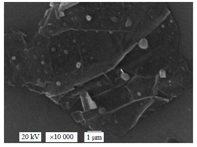
Figure 4 shows the SEM image of the fabricated graphene functional layer. Due to the coarse nature of the coating procedure,the graphene flakes overlapped irregularly,and film thickness ranged from hundreds of nanometers to a few micrometers. This morphology was consistent with the previous results of the slightly lower transmittance in Fig. 3. It also can be seen that,the graphene cluster consisted of a number of sheet-like structures. Making use of these blade-like edges with atomic thickness,it could greatly increase the electric field enhancement factor.

Figure 4. SEM image of graphene functional layer coated on silicon substrate by spraying of graphene solution (15 wt % SDBS)
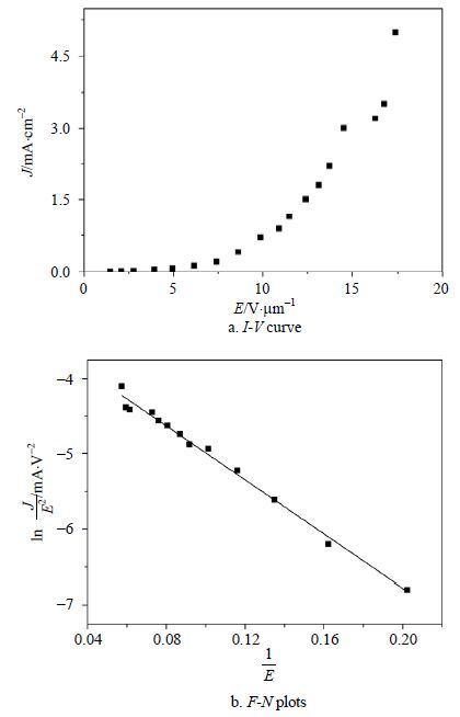
Figure 5a shows the field emitting current density-voltage (J-V) characteristics of graphene functional layer coated on silicon substrate at 6×10⁻⁵ Pa in diode geometry. With the increase of anode voltage,the emission current density increased very rapidly,finally reached 5 mA/cm2 at electric field of 17.5 V/μm. Furthermore,it exhibited a low turn-on field of 3 V/μm,which was well comparable to other cold cathodes,including a Si nanotip array of 8.5 V/μm[16] and CNT field emitters of 2~5 V/μm[17]. We suggested that this satisfactory field emitting performance of graphene film was not only due to its unique high aspect ratio but also due to its special appearance presented in the SEM photograph (Fig. 4) . As shown in Fig. 4,graphene films were made of flat graphene sheets laminated together. Although this flat sheet structure was contrary to conventional field-emission cathodes with sharp surface (i.e. Spindt emitters and CNTs),when there was a strong vertical electric field applied,the graphene sheets would be pulled up and more edges exposed. Owing to the special edge-field enhancing effect,lots of electrons emitted from graphene films. Moreover,because the pulled up graphene sheets were separated,the influence of electric field shielding effect may be reduced and field emitting performance would be improved further.
Figure 5b shows the Fowler-Nordheim (F-N) plots of measured graphene films. The F-N points formed a straight line approximately,which confirmed that the current was indeed the result of field emission. According to the Fowler-Nordheim theory,electric field enhancement factor ($\beta $) of emitter surface was evaluated by using the Fowler-Nordheim equation,i.e.,
$$\begin{align} & \text{ln}\left( \frac{J}{{{E}^{2}}} \right)=\text{ln}\left( 1.54\times {{10}^{-6}}\frac{{{\beta }^{2}}}{\phi {{t}^{2}}\text{(}y\text{)}} \right)+ \\ & \frac{9.87}{\sqrt{\phi }}-6.53\times {{10}^{7}}\left( \frac{{{\phi }^{3\text{/}2}}}{\beta E} \right) \\ \end{align}$$ (2) 
Figure 5. Field emitting performance of graphene functional layer coated on Si
where f is work function in eV; ${{t}^{2}}\text{(}y\text{)}$is field-dependent correction factor,which is approximated as ${{t}^{2}}\text{(}y\text{)}\approx \text{1}$for most applications; E is electric field strength in V/cm; J is field emitting current density in A/cm2. Consequently,the slope of the F-N plot in Fig. 5b was given by:
$$S\cong \text{slope=}-6.53\times {{10}^{3}}\left( \frac{{{\phi }^{3\text{/}2}}}{\beta } \right)$$ (3) Assuming that the work function of multilayer graphene films was 4.3 eV[18],the field enhancement factor of graphene film was determined to be 3 580 from the constant F-N slope. This large enhancement factor allowed for sufficient tunneling of electrons from graphene through surface barriers and resulted in the low turn-on voltage as previously described.
-
We developed a simple and practical method to obtain a graphene functional layer with remarkable field-emission performance by using the spray-coating method. The UV-vis absorption spectra for the stable graphene dispersions were measured to examine their dispersion properties. The optical transmittance and morphological of the prepared films were investigated. The results revealed that the visible light transmittance of graphene film was higher than 82% and graphene flakes overlapped irregularly on silicon substrate with numerous blade-like edges. In addition,the graphene films showed excellent field-emission properties,with low turn-on field of 3 V/μm and large enhancement factor of 3 580. These results provide a convenient approach to create new graphene-based devices.
Study on Preparation and Properties of the Graphene Functional Layer by the Spray Coating Method
-
摘要: 以十二烷基苯磺酸钠(SDBS)为表面活性剂,采用超声分散工艺制备出稳定的石墨烯水分散液,并采用喷涂法分别在玻璃和n-Si基底上形成石墨烯薄膜。研究了表面活性剂浓度对石墨烯分散效果的影响。结果表明,采用浓度为15%的SDBS可获得稳定的石墨烯水溶液分散液。利用分光光度计和扫描电镜对石墨烯薄膜的透过率和表面形貌进行表征,结果表明其可见光透过率超过82%,薄膜具有刀刃状的边缘结构。采用二极管结构对石墨烯薄膜的场发射性能进行测试,其开启电场为3V/μm,场增强因子为3 580。实验结果表明,这是一种可行的、低成本的制作石墨烯功能层的有效方法。
-
关键词:
- dispersions /
- field emission /
- graphene /
- surfactant /
- transmittance
Abstract: Stable aqueous graphene dispersion with sodium dodecyl benzene sulfonate (SDBS) surfactant was prepared by using an ultrasonic dispersing process. Graphene films were deposited on glass and silicon substrate as functional layers by the spray coating method. The study of the influence of SDBS concentration on graphene dispersing performance show that SDBS concentration of 15% is adequate for preparing stable graphene dispersion. Optical and morphological properties of the resulting graphene films are also investigated by ultraviolet-visible spectrophotometer and scanning electron microscopy, respectively. The results indicate that the visible light transmittance of graphene coating is higher than 82% and the graphene film shows a cluster structure with blade-like edges. The field emission analyses were carried out by a diode test cell in a vacuum system, which confirms that this graphene functional layer has good field-emission performance with low turn-on field of 3 V/μm and large enhancement factor of 3 580. Collectively, this deposition method may be a viable and cost-effective route for fabricating graphene films.-
Key words:
- dispersions /
- field emission /
- graphene /
- surfactant /
- transmittance
-
Figure 1. Schematic diagram of the diode configuration used for an investigation of field emitting properties of graphene films
Figure 2. UV-vis absorption spectra of graphene dispersions with different SDBS concentrations by means of ultrasonication (5 h) and centrifugal processing
Figure 3. A transmission spectrum of a graphene functional layer coated on a glass slide by spraying of graphene solution (15 wt % SDBS)
Figure 4. SEM image of graphene functional layer coated on silicon substrate by spraying of graphene solution (15 wt % SDBS)
-
[1] CANTY R, GONZALEZ E, MACDONALD C, et al. Reduction expansion synthesis as strategy to control nitrogen doping level and surface area in graphene[J]. Materials, 2015, 8(10):7048-7058. doi: 10.3390/ma8105359 [2] FAN Y, IGARASHI G, JIANG W, et al. Highly strain tolerant and tough ceramic composite by incorporation of graphene[J]. Carbon, 2015, 90:274-283. doi: 10.1016/j.carbon.2015.04.029 [3] OTHMAN M, RITIKOS R, MUHAMMAD H, et al. Low-temperature plasma-enhanced chemical vapour deposition of transfer-free graphene thin films[J]. Materials Letters, 2015, 158:436-438. doi: 10.1016/j.matlet.2015.06.039 [4] VAIANELLA F, ROSOLEN G, MAES B. Graphene as a transparent electrode for amorphous silicon-based solar cells[J]. Journal of Applied Physics, 2015, 117(24):243102. doi: 10.1063/1.4923232 [5] ERVIN M H. Etching holes in graphene supercapacitor electrodes for faster performance[J]. Nanotechnology, 2015, 26(23):234003. doi: 10.1088/0957-4484/26/23/234003 [6] LAI L, YANG H, WANG L, et al. Preparation of supercapacitor electrodes through selection of graphene surface functionalities[J]. ACS Nano, 2012, 6(7):5941-5951. doi: 10.1021/nn3008096 [7] VADIVAAMBIGAI A, SENTHILVASAN P A, KOTHURKAR N, et al. Graphene-oxide-based electro chemical sensor for salicylic acid[J]. Nanoscience and Nanotechnology Letters, 2015, 7(2):140-146. doi: 10.1166/nnl.2015.1909 [8] LEE J S, OH J, JUN J, et al. Wireless hydrogen smart sensor based on Pt/graphene-immobilized radio-frequency identification tag[J]. ACS Nano, 2015, 9(8):7783-7790. doi: 10.1021/acsnano.5b02024 [9] EDA G, FANCHINI G, CHHOWALLA M. large area ultrathin films of reduced graphene oxide as a transparent and flexible electronic material[J]. Nature Nanotechnology, 2008, 3(5):270-274. doi: 10.1038/nnano.2008.83 [10] GUO Y L, DI C A, LIU H T, et al. General route toward patterning of graphene oxide by a combination of wettability modulation and spin-coating[J]. ACS Nano, 2010, 4(10):5749-5754. doi: 10.1021/nn101463j [11] ARAPOV K, GORYACHEV A, WITH G D, et al. A simple and flexible route to large-area conductive transparent graphene thin-films[J]. Synthetic Metals, 2015, 201:67-75. doi: 10.1016/j.synthmet.2015.01.016 [12] WU Z S, PEI S F, REN W C, et al. Field emission of single-layer graphene films prepared by electrophoretic deposition[J]. Advanced Materials, 2009, 21:1756-1760. doi: 10.1002/adma.v21:17 [13] DENG J, ZENG B Q, WANG X J, et al. Lowering of the firing voltage and reducing of the discharge delay time in alternating current plasma display panels by a discontinuous spin-coated LaB6 film on the MgO protective layer[J]. AIP Advance, 2014(4):037109. http://cn.bing.com/academic/profile?id=29f4fc9eba6eda4411d870681054ab8a&encoded=0&v=paper_preview&mkt=zh-cn [14] OSTFELD A E, CATHELINE A, LIGSAY K, et al. Single-walled carbon nanotube transparent conductive films fabricated by reductive dissolution and spray coating for organic photovoltaics[J]. Applied Physics Letters, 2014, 105:253301. doi: 10.1063/1.4904940 [15] LI D, MÜLLER M B, GILJE S, et al. Processable aqueous dispersions of graphene nanosheets[J]. Nature Nanotechnology, 2008, 3(2):101-105. doi: 10.1038/nnano.2007.451 [16] HUANG G S, WU X L, CHENG Y C, et al. Fabrication and field emission property of a Si nanotip array[J]. Nanotechnology, 2006, 17:5573-5576. doi: 10.1088/0957-4484/17/22/008 [17] JUNG M S, KO Y K, JUNG D H, et al. Electrical and field-emission properties of chemically anchored single-walled carbon nanotube patterns[J]. Appied Physics Letters, 2005, 87:013114. doi: 10.1063/1.1968430 [18] PARK S J, PARK H, LEE Y, et al. Increasing the effective work function of multilayer rapheme films using silver nanoparticles[J]. Journal of Vacuum Science and Technology B, 2014, 32(1):011214. doi: 10.1116/1.4861372 -

 点击查看大图

计量
- 文章访问数: 3930
- HTML全文浏览量: 1160
- PDF下载量: 48
- 被引次数: 0