ISSN
ISSN 


-
Compared with traditional thermionic cathode, field emission array cathode (FEAs) has several advantages, such as low operating temperature, strong controllability, large emission current, and short response time. It has attracted extensive attention in the applications of high-frequency devices, flat panel displays, x-ray tube, and so on[1-4]. Take the field emission traveling wave tubes (TWTs) as an example. Firstly, it can work at room temperature without any heating equipment, resulting in low power consumption. Secondly, it is very easy to adjust emission current by changing the gate voltage, showing excellent switching characteristics and extremely high response speed. Reference [5] have reported the experimental results of implementation of Mo-FEA as the electron source for a moderate power traveling wave tube operating in the C-band frequency regime. The cold cathode TWT has operated for over 150 h at duty factors up to 10% and beam currents up to 121 mA. Although field emission cathode has made great progress in recent years, there are also some problems in the practical applications, mainly including its emission instability[6-9]. The possible reason for the emission instability is that it is very difficult to prepare millions of microtips with the same shape on a silicon substrate. Thus, searching new materials and developing novel structures for field emission arrays are urgently needed.
A few novel structures of FEAs have been fabricated and shown enhanced performance in some papers. References [10-11] fabricated mesh shaped resistor layers in a FEA, and Ref.[12] manufactured Spindt FEA with distributed series resistors. Both of them confirmed that the resistor grid layers may favorably improve the performance of an FEA. In addition, Ref.[13] reported a Spindt-type FEA with lanthanum hexaboride (LaB6) as the emitting material. It exhibited an average emission current as high as about 0.23 A/tip, implying that LaB6 emitter was a promising candidate for high current density vacuum electronic device.
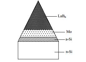
In this work, a novel structure of Spindt-FEA was proposed. It included three layers: amorphous silicon (a-Si) film as a resistance layer, molybdenum (Mo) film as a transition layer, and LaB6 film as an emission layer. The amorphous silicon film could effectively limit the abnormal emission of some microtips, which played a role in protecting the entire field emission cathode array. Molybdenum film connected amorphous silicon and LaB6 film through its suitable thermal expansion coefficient, improving the working stability of FEAs. LaB6 emitter was introduced to enhance the emission performance of cathodes, owing to its low work function and excellent mechanical stability against ion bombardment. Considering the thermal stress caused by the above three layers stacking, the finite element analysis software ANSYS14.0 was used to simulate the influence of each layer thicknesses on the distribution of thermal stress field of the cathode. The optimal structural parameters were obtained, and the accuracy of the simulation results was verified by a DTI-500 thermal stress meter.
-
Figure 1 shows the two-dimensional plane mathematical model of the cathode used in our simulation. Firstly, the thickness of the resistive layer was studied, which seriously affected the emission current of the cathode. According to the literature[13], the emission current of LaB6-FEA single tip was about 0.24 μA at gate voltage of 165 V. Thus, assuming that with the addition of the resistive layer, the gate voltage was reduced by 25%, 30%, 35%, and 40%, and the thickness of the resistive layer could be calculated as 45, 54, 63 and 72 nm respectively on the basis of Ohm's law and resistance formula. In addition, the thickness of the transition layer was set to 0, 0.1, 0.2, 0.3 and 0.4 μm, respectively. The height of silicon substrate and the whole tip were both fixed at 1 μm.

Figure 1. Simulation model of LaB6 composite field emission array cathode
Next, the working temperature of LaB6 composite field emission array was needed to be confirmed and turned into mathematical language for ANSYS simulation. Because the bottom size and height of the cathode were both in the micron level, the operating temperature was set to steady-state temperature field, that is, the temperature of any point in the cathode did not change with time. In addition, only heat conduction was considered in the heat transferring process, ignoring the thermal convection and thermal radiation.
During the simulation, it was assumed that the material parameters of cathode (lanthanum hexaboride, molybdenum, amorphous silicon and silicon substrate) did not change with the temperature, so there was no need to define the function of material properties and temperature. Four material parameters associated with thermal analysis were defined: thermal conductivity, elastic modulus, coefficient of thermal expansion, and Poisson's ratio, as shown in Table 1[14].
Table 1. Material parameters of Spindt cathode
Each layer Thermal conductivity/ W·m-1·K Elastic modulus /Gpa Coefficient of thermal expansion /10-6·k-1 Poisson's ratio n-Si (substrate) 150 170 2.5 0.3 a-Si (resistive layer) 1.5 360 3.6 0.278 Mo (transition layer) 138 330 5.3 0.3 LaB6 (emission layer) 45 160 6.5 0.3 -
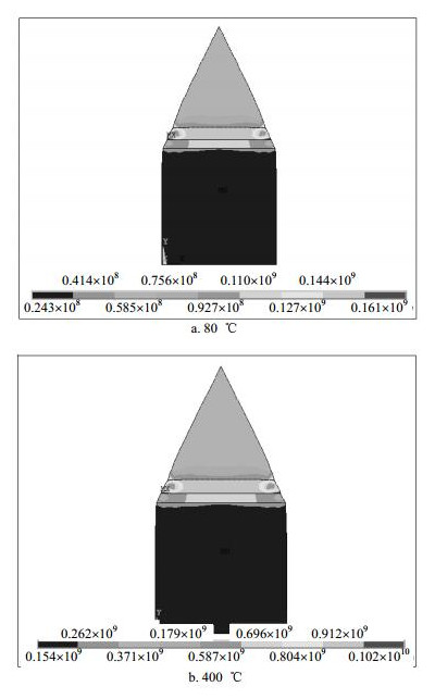
Figure 2 compares the results of the stress simulation of the cathodes at loading temperatures of 80 ℃ and 400 ℃, respectively. It is found that the loading temperature variation has little effect on the thermal field distribution of the model. The maximum stress of both cathodes appear at the center of the molybdenum layer, with the value of 1.54×10⁸ Pa and 9.8x10⁸ Pa, respectively. In our experiment, the thermal field distribution is the focus. Thus, the loading temperature of the cathode is set to 80 in the next simulation.

Figure 2. Thermal stress distribution of the cathode at different loading temperatures
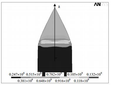
Figure 3 shows the thermal stress distribution of the cathode without a resistive layer and transition layer. The maximum stress up to 8.2×10⁷ Pa appears at the emission layer, which is harmful to the working stability of the emitter.

Figure 3. Thermal stress distribution of the cathode without a resistive layer and transition layer
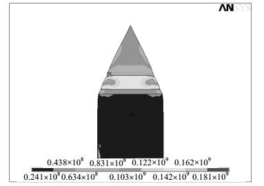
Figure 4 shows the thermal stress field of the model without a transition layer (h2=0 nm). The thickness of the resistive layer (h1) is 45 nm and the height of the emitter is 0.955 μm. The equivalent stress distribution of the cathodes with different thickness of resistive layer is similar. It indicates that, when there is no transition layer, the maximum value of the thermal stress appears at the interface between the emission layer and the resistance layer.

Figure 4. Thermal stress distribution of the cathode without a transition layer (h1=45 nm)
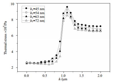
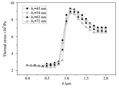
Figure 5 shows the corresponding thermal stress values of the model without a transition layer. The abscissa (h) represents the distance between the points on the center axis of the model and the center of substrate bottom, as shown in Figure 4. It is found that no matter how thick the resistive layer is, the maximum thermal stress always appears at the interface between the emissive layer and the resistive layer. However, with the increase of the thickness of resistive layer, the maximum thermal stress is obviously reduced. In addition, the thermal stress of the emissive layer always keeps at a high value (8.0×10⁷~9.1×10⁷ Pa).

Figure 5. Thermal stress of the cathode at h2=0 nm
Figure 6 shows the thermal stress in the model when the thickness of transition layer is 0.1 μm. Compared with Figure 5, the simulation results show obvious changes with the addition of the transition layer. Firstly, the position of the maximum stress in the model changes to the interface between the transition layer and the emission layer. Secondly, the thermal stress value of emission layer is obviously lower than that of h2=0 μm, which is about 6.5×10⁷~7.8×10⁷ Pa. It indicates that, the molybdenum transition layer indeed has an effect on alleviating the thermal stress of the emission layer, acting as a gradient role in the model. However, unfortunately the large stress at the interface leads to the deformation of the transition layer or/and the emission layer, which is bad for the operation stability of the cathode. Thus we can conclude that the parameter of h2=0.1 μm does not meet the expected design requirements.

Figure 6. Thermal stress of the cathode at h2=0.1
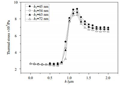
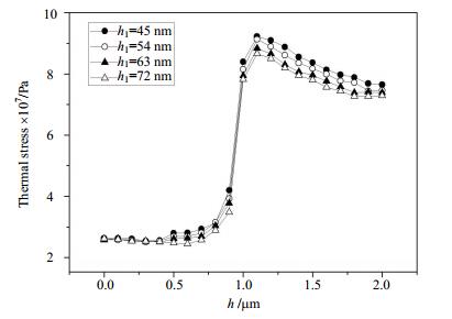
Figure 7 shows the thermal stress in the model when the thickness of transition layer is 0.2 μm. Regardless of the thickness of the resistive layer, the maximum thermal stress appears inside the transition layer. Compared with the results of h2=0.1 μm, the thermal stress of the emission layer decreases slightly, which is about 6.4×10⁷~7.7×10⁷ Pa. The above two features are beneficial to the cathode stability. Moreover, as the thickness of the resistive layer increases, the maximum value of the thermal stress is smaller. For example, when the thickness of the resistance layer increases from 45~72 nm, the maximum thermal stress decreases by 0.6×10⁷ Pa. It is known that, the smaller the thermal stress is, the more stably the cathodes work. Thus, we can conclude that when the transition layer is 0.2 μm and the resistance layer is 72 nm, the simulation results are ideal and the thermal stress distribution of the cathode is shown in Figure 8.

Figure 7. Thermal stress of the cathode at h2=0.2 μm

Figure 8. Thermal stress distribution of the cathode at h1=0.072 μm, h2=0.2 μm
Figure 9 and Figure 10 show the thermal stress in the model when the thickness of transition layer is 0.3 μm and 0.4 μm, respectively. Compared with the results of h2=0.2 μm model, the thermal stress of the emission layers in Fig. 9 and Fig. 10 both increases slightly. All the maximum stress values appear at the interface between the a-Si film and Mo film, which may cause the resistance layer to deform or fall off, and result in operation instability of the cathode.

Figure 9. Thermal stress of the cathode at h2=0.3 μm

Figure 10. Thermal stress of the cathode at h2=0.4 μm
-
According to the simulation results, the optimum parameters are as follows: a-Si layer thickness is 72 nm, Mo layer thickness is 200 nm, and LaB6 layer thickness is 728 nm. The above parameters were experimentally verified in our paper. Firstly, a-Si film with thickness of ~75 nm was deposited on n-Si substrate, and followed by LaB6 film with thickness of ~750 nm. Then another three-layer structure was also prepared, which included a-Si layer (~75 nm thickness), Mo layer (~205 nm thickness) and LaB6 layer (~750 nm thickness) in turn. The thermal stress of the above two structures were tested by a thermal stress meter.
Table 2 and Table 3 show the results of thermal stress analysis of the double and triple films, respectively. When there is no molybdenum transition layer (Tab. 2), the thermal stress of amorphous silicon layer is much larger than that of lanthanum hexaboride layer, which is consistent with the simulation results in Fig. 5 (h1=72 nm).The average thermal stress of the amorphous silicon layer and the lanthanum hexaboride layer in Fig. 5 (h1=72 nm) are calculated to be 8.5×10⁷ Pa and 8.3×10⁷ Pa, respectively, which are slightly lower than the test results.
Table 2. Thermal stress test results of a-Si-LaB6 double films
Parameters a-Si layer LaB6 layer Film thickness/nm 75 750 Thermal stress×107/Pa 9.0 8.4 Table 3. Thermal stress test results of a-Si-Mo-LaB6 triple films
Parameters a-Si layer Mo layer LaB6 layer Film thickness/nm 75 205 750 Thermal stress×107/Pa 7.8 9.3 6.2 On the other hand, when the molybdenum transition layer is added (Tab. 3), the maximum thermal stress value appears in the molybdenum film layer, which is consistent with the simulation curve in Fig. 7 (h1=72 nm). Compared with the data in Tab. 2, the thermal stress of the lanthanum hexaboride layer is greatly reduced, confirming that the molybdenum transition layer does have an effect on alleviating the thermal stress of the emission layer. In addition, the average thermal stresses of the amorphous silicon layer, molybdenum layer, and lanthanum hexaboride layer in Fig. 7 (h1=72 nm) are 8.0×10⁷, 8.5×10⁷and 6.6×10⁷ Pa, respectively. The possible reason for the thermal stress difference between the measurement and simulation results is that, the simulation result is the average stress under the ideal parameters of each layer, while the test value is the single experimental result. However, it should be noted that, the experimental value of thermal stress is less than 10% compared with the simulation result, which is within the allowable range.
-
In conclusion, the influence of the thickness of each layer of LaB6 composite field emission array on the thermal stress has been simulated based on the ANSYS platform. The optimal structural parameters are determined and verified by experiments, and the following conclusions are obtained:
1) The thickness of resistive layer does not affect the distribution of the thermal stress field, but the maximum value of the thermal stress decreases with the increase of resistive layer thickness.
2) The introduction of the transition layer has a significant effect on reducing the thermal stress of the emission layer.
3) The simulation results show that the optimum structural parameters of the cathode are as follows: the thickness of the resistive layer is 72 nm, the thickness of the transition layer is 200 nm, and the thickness of the emitter layer is 728 nm.
4) The thermal stress test results are consistent with the simulation results, which confirm the importance of molybdenum film for improving the stability of the cathode.
-
摘要: 为了提高传统Spindt型场发射阵列阴极的稳定性,提出了一种新型的LaB6复合型场发射阵列阴极结构,该结构包括非晶硅电阻层、钼过渡层和六硼化镧发射体层。基于ANSYS平台模拟了该阴极中电阻层、过渡层和发射体层厚度对热应力场分布的影响,并根据仿真结果进行了实验验证。仿真结果表明,电阻层厚度不影响热应力场的分布,只是改变热应力的大小;随着电阻层厚度的增加,阴极最大热应力会减小;过渡层可以有效减缓发射层的热应力,且过渡层的厚度会影响热应力场的分布;当电阻层厚度为72 nm,过渡层厚度为200 nm,发射层厚度为728 nm时,阴极最为稳定。薄膜热应力测试结果与模拟结果基本一致,证实了引入过渡层和电阻层对于减小阴极热应力的可行性。Abstract: In order to improve the operation stability of traditional Spindt field emission array cathode, a novel structure of lanthanum hexaboride (LaB6) composite field emission array cathode is proposed, which includes an amorphous silicon resistance layer, a molybdenum transition layer, and a lanthanum hexaboride emitter layer. The influences of the thickness of the resistive layer, the transition layer, and the emitter layer on the thermal stress field distribution of the cathode are simulated by ANSYS and the results of simulation are verified by experiments. Simulation results show that the thickness of the resistive layer does not affect the distribution of the thermal stress field, but only changes the value of the thermal stress. The maximum thermal stress of the cathode decreases as the thickness of the resistive layer increases. The transition layer can effectively alleviate the thermal stress of the emission layer, and its thickness affects the field distribution of thermal stress. As a result, the optimum parameters are as follows:a-Si layer thickness is 72 nm, Mo layer thickness is 200 nm, and LaB6 layer thickness is 728 nm. The thermal stress test results of the films are consistent with the simulation results, which proves the feasibility of reducing the thermal stress by introducing the transition layer and the resistive layer.
-
Key words:
- ANSYS /
- field emission array /
- emission layer /
- resistive layer /
- transition layer
-
Figure 2. Thermal stress distribution of the cathode at different loading temperatures
Figure 3. Thermal stress distribution of the cathode without a resistive layer and transition layer
Figure 4. Thermal stress distribution of the cathode without a transition layer (h1=45 nm)
Table 1. Material parameters of Spindt cathode
Each layer Thermal conductivity/ W·m-1·K Elastic modulus /Gpa Coefficient of thermal expansion /10-6·k-1 Poisson's ratio n-Si (substrate) 150 170 2.5 0.3 a-Si (resistive layer) 1.5 360 3.6 0.278 Mo (transition layer) 138 330 5.3 0.3 LaB6 (emission layer) 45 160 6.5 0.3  下载: 导出CSV
Table 2. Thermal stress test results of a-Si-LaB6 double films
Parameters a-Si layer LaB6 layer Film thickness/nm 75 750 Thermal stress×107/Pa 9.0 8.4
下载: 导出CSV
Table 3. Thermal stress test results of a-Si-Mo-LaB6 triple films
Parameters a-Si layer Mo layer LaB6 layer Film thickness/nm 75 205 750 Thermal stress×107/Pa 7.8 9.3 6.2
下载: 导出CSV
-
[1] CHEN J T, YANG B Q, LIU X H, et al. Field electron emission from pencil-drawn cold cathodes[J]. Applied Physics Letters, 2016, 108(19):193112. doi: 10.1063/1.4949563 [2] XU J Z, XU P, OU-YANG W, et al. Outstanding field emission properties of wet-processed titanium dioxide coated carbon nanotube based field emission devices[J]. Applied Physics Letters, 2015, 106(7):073501. doi: 10.1063/1.4909552 [3] KIM H S, CASTRO E J D, LEE C H. Optimum design for the carbon nanotube based micro-focus x-ray tube[J]. Vacuum, 2015, 111:142-149. doi: 10.1016/j.vacuum.2014.10.009 [4] QIN F, WANG D, XU S, et al. Repetitive operation of an L-band magnetically insulated transmission line oscillator with metal array cathode[J]. Review of Scientific Instruments, 2016, 87:044101. doi: 10.1063/1.4945113 [5] WHALEY D R, BELLEW C L, SPINDT C A. 100 W operation of a cold cathode TWT[J]. IEEE Transactions on Electron Devices, 2009, 56(5):896-905. doi: 10.1109/TED.2009.2015614 [6] SCHEOEBEL P R, BRODIE I. Surface-science aspect of vacuum microelectronics[J]. Journal of Vacuum Science and Technology, 1995, B13(4):1391-1410. doi: 10.1116/1.584597 [7] CHALAMALA B R, REUSS R H. Studies on the interaction between thin film materials and Mo field emitter arrays[J]. Journal of Vacuum Science and Technology, 2000, B18(4):1825-1832. doi: 10.1116/1.1303755 [8] FENG J J. Stability of field emitter array in microwave tubes[J]. Journal of Vacuum Science and Technology, 2005, 25:16-19. https://www.researchgate.net/publication/289165927_Stability_of_field_emitter_array_in_microwave_tubes [9] YUAN J, DU B C, LI D J. Analysis on degradation mechanism in emission current of field-emitter array[J]. Microfabrication Technology, 2002, 3:70. https://www.researchgate.net/publication/293260049_Analysis_on_degradation_mechanism_in_emission_current_of_field-emitter_array [10] QU X S, LI D J, YAO B L. Influence of mesh shaped resistive layers on field emission arrays[J]. Journal of Vacuum Science and Technology, 2000, 20(4):229-231. https://www.researchgate.net/publication/293262618_Study_on_metal_field_emission_array [11] QU X S, LI D J, YAO B L. The distribution resistor layer on FEA[J]. Semiconductor Optoelectronics, 2000, 21(3):196-202. http://en.cnki.com.cn/Article_en/CJFDTotal-BDTG200003013.htm [12] WANG W, LI D J, YAO B L, et al. Research on Spindt FEA with distributed series lateral resistor layer[J]. Microfabrication Technology, 2000(2):13-18. doi: 10.1143/JJAP.41.301 [13] QI K C, LIN Z L, CHEN W B, et al. Formation of extremely high current density LaB6 field emission arrays via e-beam deposition[J]. Applied Physics Letters, 2008, 93:093503. doi: 10.1063/1.2977616 [14] CHO J R, TINSLEY O J. Functionally graded material:a parametric study on thermal-stress characteristics using the Crank-Nicolson-Galerkin scheme[J]. Comput Methods Appl Mech Engrg, 2000, 188:17-38. doi: 10.1016/S0045-7825(99)00289-3 -

 点击查看大图
计量
- 文章访问数: 3725
- HTML全文浏览量: 1111
- PDF下载量: 84
- 被引次数: 0