 ISSN
ISSN 


-
科学技术的快速发展使得电子产品的性能飞速提高。传统硅基器件的性能被不断挖掘,在许多领域都表现得十分优异。但是由于其材料自身的物理特性,属于刚性材质[1],限制了其在柔性电子领域的应用。传统电子器件的柔韧性以及可延展性非常有限,无法满足未来电子领域的柔性化发展需求。
相对于传统的硅材料而言,二维材料有其独特的优势。此类材料可以通过将大块材料剥离成小尺寸获得[2],或通过化学气相沉积(Chemical Vapor Deposition, CVD)获得大面积[3]。并且其原子级薄的单层或几层晶体具有强的层内共价键和弱的层间范德瓦尔斯键,从而具有优异的电学、光学和机械性能[4-6]。同时,二维材料中有半导体,导体,绝缘体,使得二维材料在柔性电子领域具有非常大的研究潜力和应用价值。
二维材料具有高的机械拉伸强度[7-8]以及光学透明度,并表现出非常优异的电荷传输性质。以石墨烯(graphene)为例,极高的杨氏模量((1.0±0.1) TPa)[9]、极高的载流子迁移率(15000 cm2/(V·s))[10],是商用硅材料迁移率的140倍。但是由于其零带隙,导致使用graphene作为沟道材料的晶体管有非常严重的漏电现象而导致极低的开关比,限制了其在晶体管领域的应用。虽然graphene作为沟道材料存在上述问题,但其超高的迁移率使得电阻非常小,可以较好地作为二维电极。而二维过度金属硫化物(TMDCs)恰好能够弥补graphene零带隙的缺点,例如,单层的二硫化钼(MoS2)的禁带宽度为1.9 eV[11-12],可以作为沟道材料。除此之外,二维材料中还有禁带宽度较大的材料可以作为绝缘体材料,例如六方氮化硼(h-BN),属于宽禁带半导体(5.0 eV~6.0 eV),可以作为栅介质层或者保护层[13-14]。
由此,本文使用graphene,MoS2,h-BN在聚对苯二甲酸乙二醇酯(Polyethylene Terephthalate, PET)上制备了基于二硫化钼的柔性场效应晶体管。同时,采用柔性测试平台,测试了器件的柔性电学特性。
-
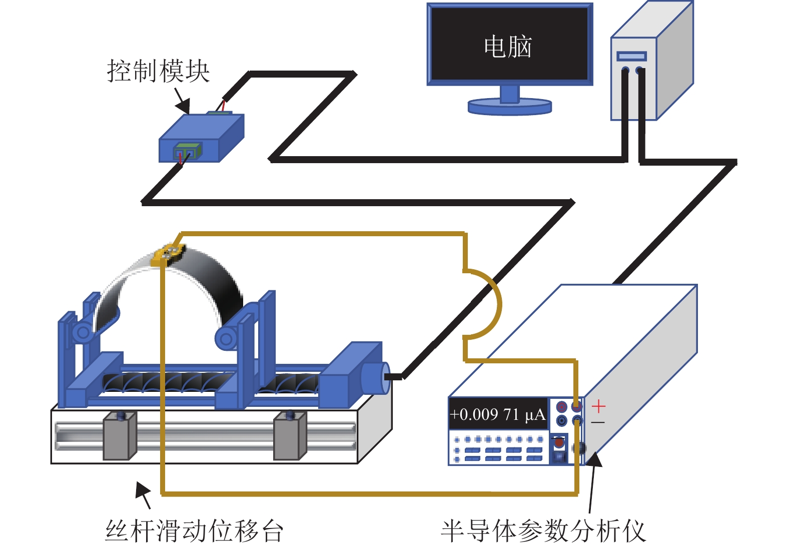
本文提出了新型柔性测试平台设计,如图1所示。该测试平台主要由丝杆滑动位移台,半导体参数分析仪,电脑,控制模块组成。柔性测试平台主要的功能分为两部分:1)通过电脑程序对控制模块进行调控,能够控制丝杆滑动位移台运动距离,运动速度,运动次数;2)通过电脑程序可以直接控制半导体参数分析仪,也可以读取半导体参数分析仪的测试数据。
相较于将柔性样品贴合至不同半径圆柱上的弯曲测试方法,本测试平台在放置样品后,能一次性测试所有不同曲率状态下器件的电学性能,无需更换不同曲率的圆柱,可以避免损坏样品。此外,采取步进电机驱动位移块的方式,改变器件的曲率,使得能够测试器件动态弯曲过程中的动态响应。
-
本文对器件的机械性能测试分为两部分:1)静态测试;2)动态测试。首先介绍静态测试设置:在这一测试条件下,丝杆滑动位移台丝杆滑动位移台(图1)最右侧为起始点,设置位移台初始运动距离为0.4 cm,同时以0.4 cm/s的速度匀速向左运动,位移台达到设定位置后,停止并保持静止不动。对器件进行电学测试,测试完毕后,位移台以相同的速度返回起始点。整个静态测试过程,位移台的位移距离从0 cm开始,每次测试位移距离增加0.4 cm,直到位移距离达到4 cm。

动态测试设置:丝杆滑动位移台最右侧为起始点,设置位移台初始速度为0.8 cm/s,位移距离为4 cm,位移台达到设定位置后,立即反向以相同的速度反向运动至起始点,此为位移台的1个周期运动,每次动态测试需要完整测试5个周期。同时进行电学测试,整个动态测试过程,位移台的运动速度从0 cm/s开始,每次测试运动速度增加0.8 cm/s,直到运动速度达到4 cm/s,保持位移距离为4 cm。
-
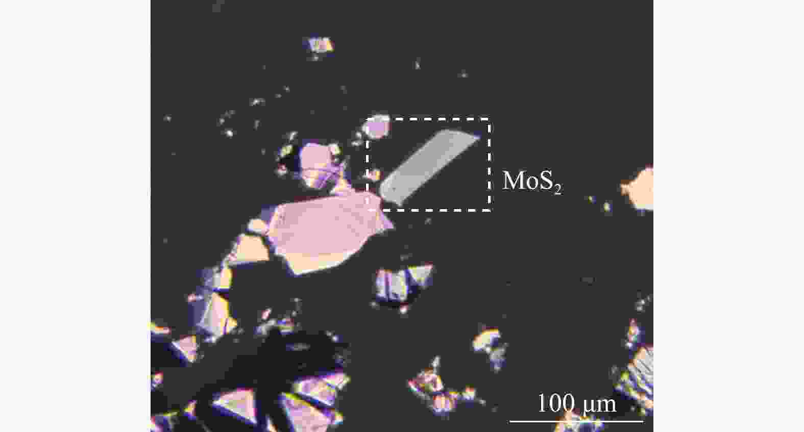
机械剥离法是最早制备薄层二维层状材料的方法之一[15-16]。二维材料层与层之间的范德瓦尔斯力较弱,可以使用粘附性较大的媒介物(胶带),对材料进行拉扯,打破材料之间范德瓦尔斯力束缚,形成薄层的二维材料。机械剥离法制备的二维材料缺陷少,材料不会被污染,同时方法简单,不需要复杂的设备。与此同时,这种方法在制备大尺寸的单层材料时,效率较为有限,同时制备的材料的尺寸不一,因此更适用于实验室中的探索性研究。
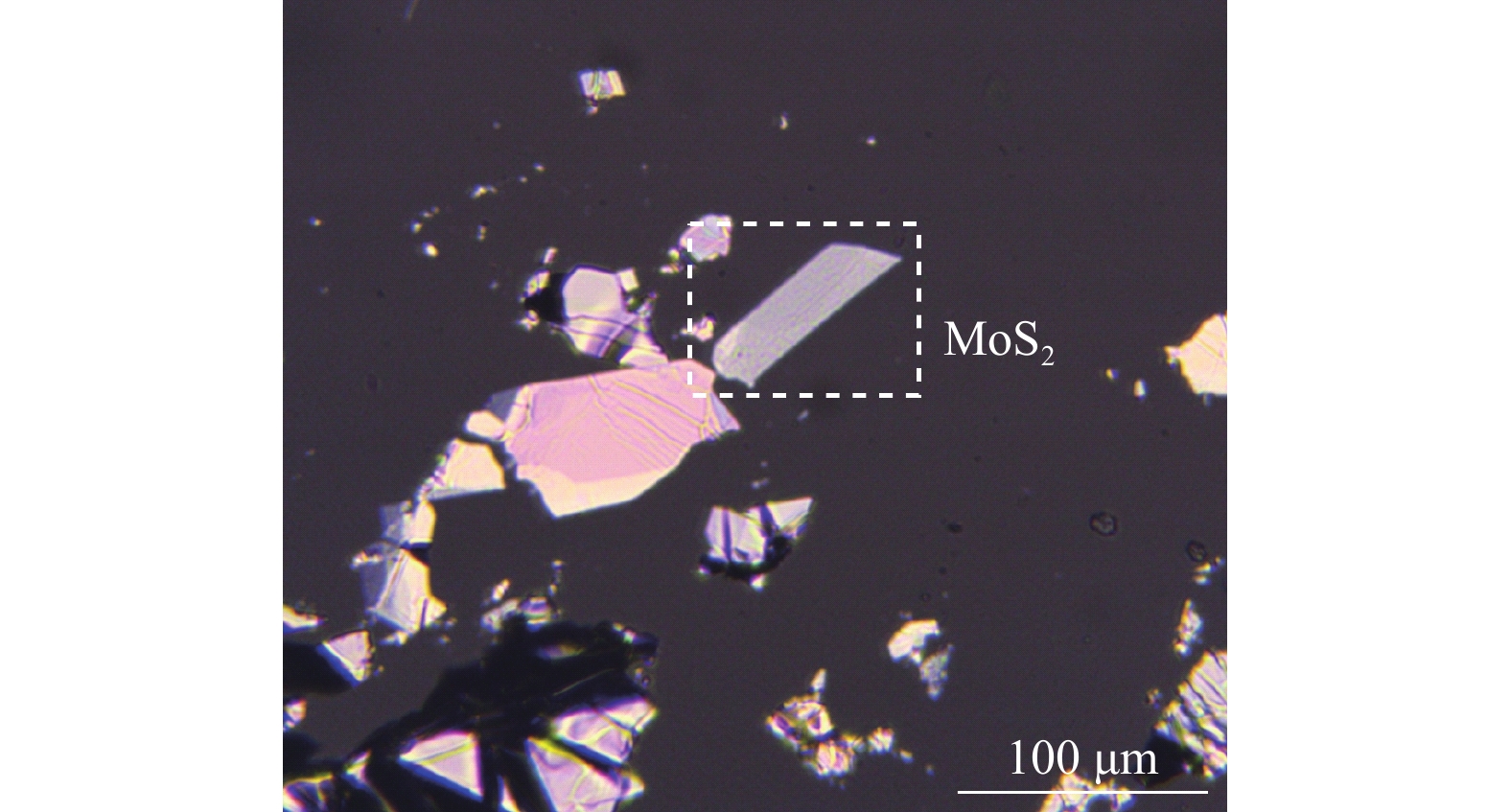
具体的实施步骤如下:1)将所要剥离的块状二维材料放置于透明胶带上;2)进行反复黏贴剥离该块体状材料,使其变为薄层材料;3)使用聚二甲基硅氧烷(Polydimethylsiloxane,PDMS)在透明胶带上粘取薄层材料;4)在光学显微镜下寻找单层或者多层的二维薄层材料,图2为光学显微镜下的薄层MoS2。
-
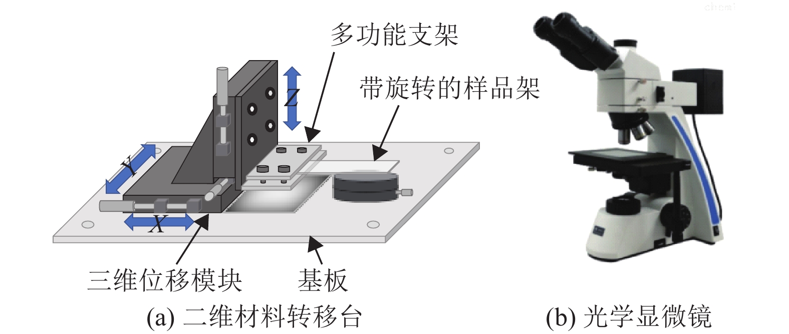
二维材料的转移可以分为干法转移与湿法转移,其中干法转移利用聚二甲基硅氧烷(Polydimethylsiloxane, PDMS)作为辅助,依靠材料与衬底之间的范德瓦尔斯力,把材料转移至衬底上[17-18]。无需使用化学试剂,材料不会受到污染。整个干法转移仅需要两个设备,如图3所示,图3a为二维材料的转移台,图3b为光学显微镜。二维材料的转移台由3部分组成:1)多功能支架能够固定载玻片;2)旋转样品台,能够调整衬底的方位,此外还可以添加半导体制冷片,进行温度调节;3)三维移动模块,能够在X、Y、Z方向微调支架位置。整个二维材料转移系统设备简单,容易操作。
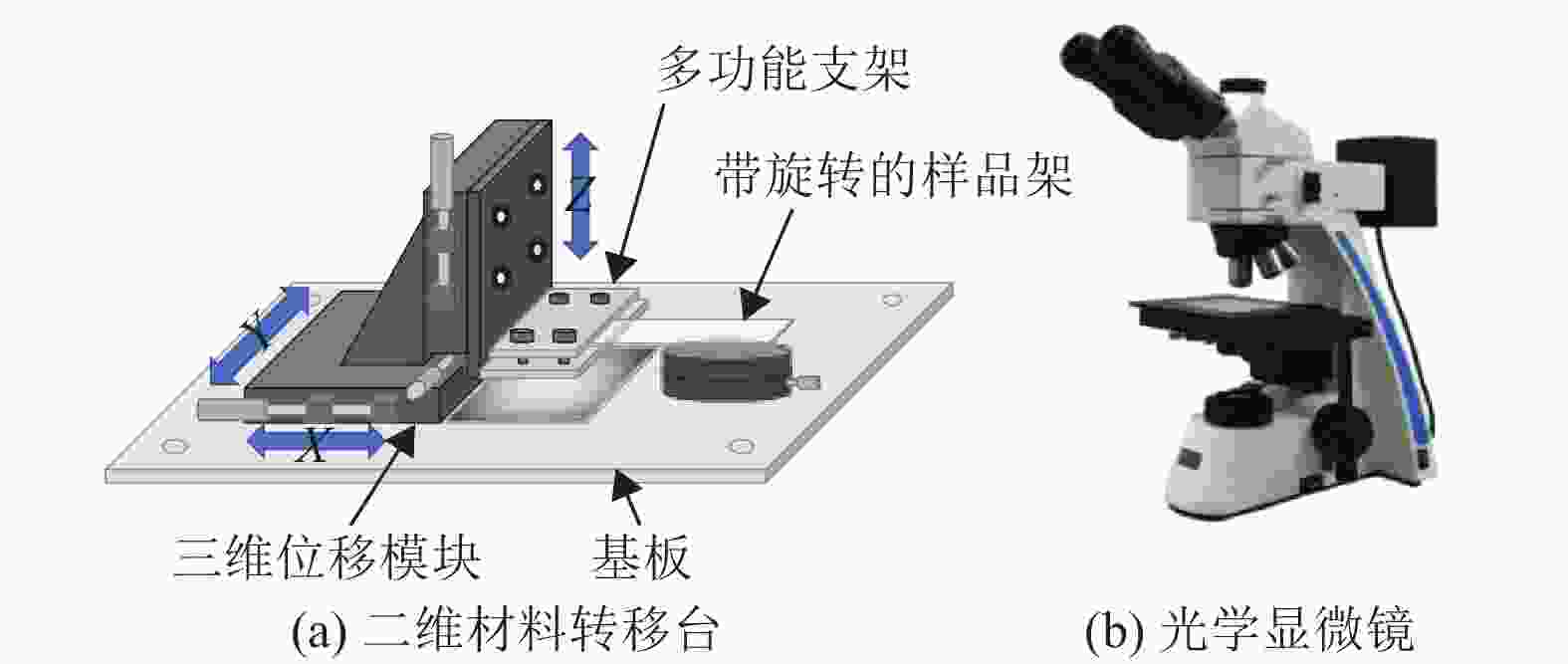
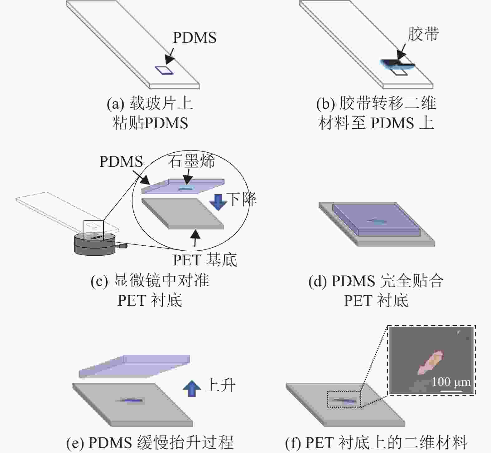
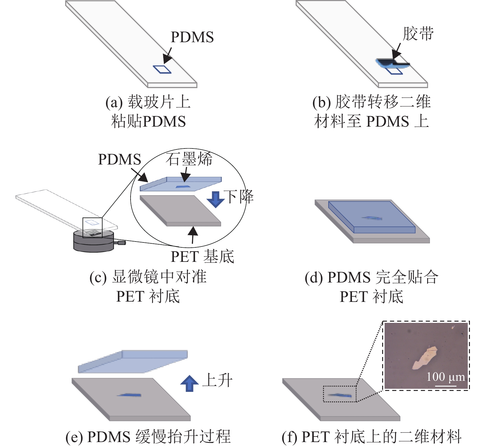
图4为基于PDMS的干法转移示意图,其具体过程为:首先,在载玻片上放置PDMS,并用其拾取机械剥离法制备的薄层材料,如图4a与图4b所示;然后,倒置放在转移台上,在光学显微镜中,观察PDMS上薄层材料与衬底的相对位置关系,同时下降载玻片,直到完全与衬底贴合,如图4c与4d所示;最后,缓慢提取载玻片,如图4e所示。由于二维材料与衬底之间存在范德瓦尔斯力,所以二维材料会留在衬底表面,如图5f所示。该方法操作简单,不使用化学试剂,不会污染材料。但是,若衬底表面存在灰层,材料转移的效率会降低。可以使用清洗衬底的方式去除表面灰层,从而提高转移成功率。
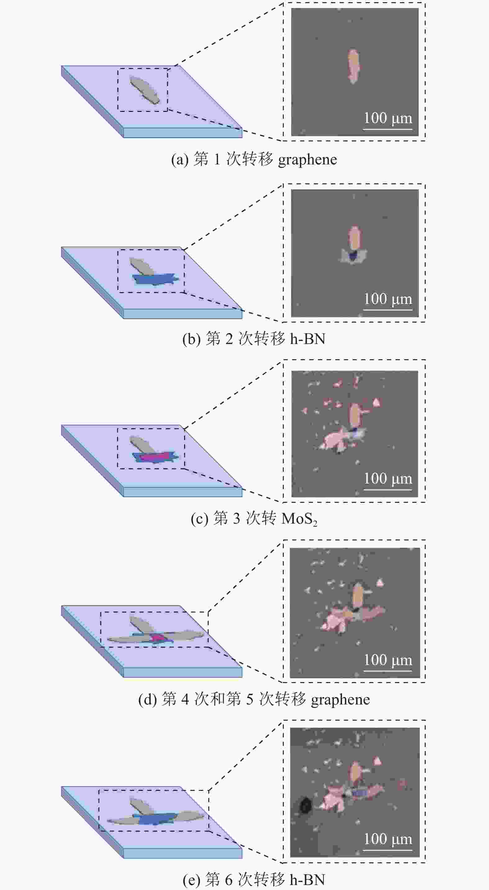
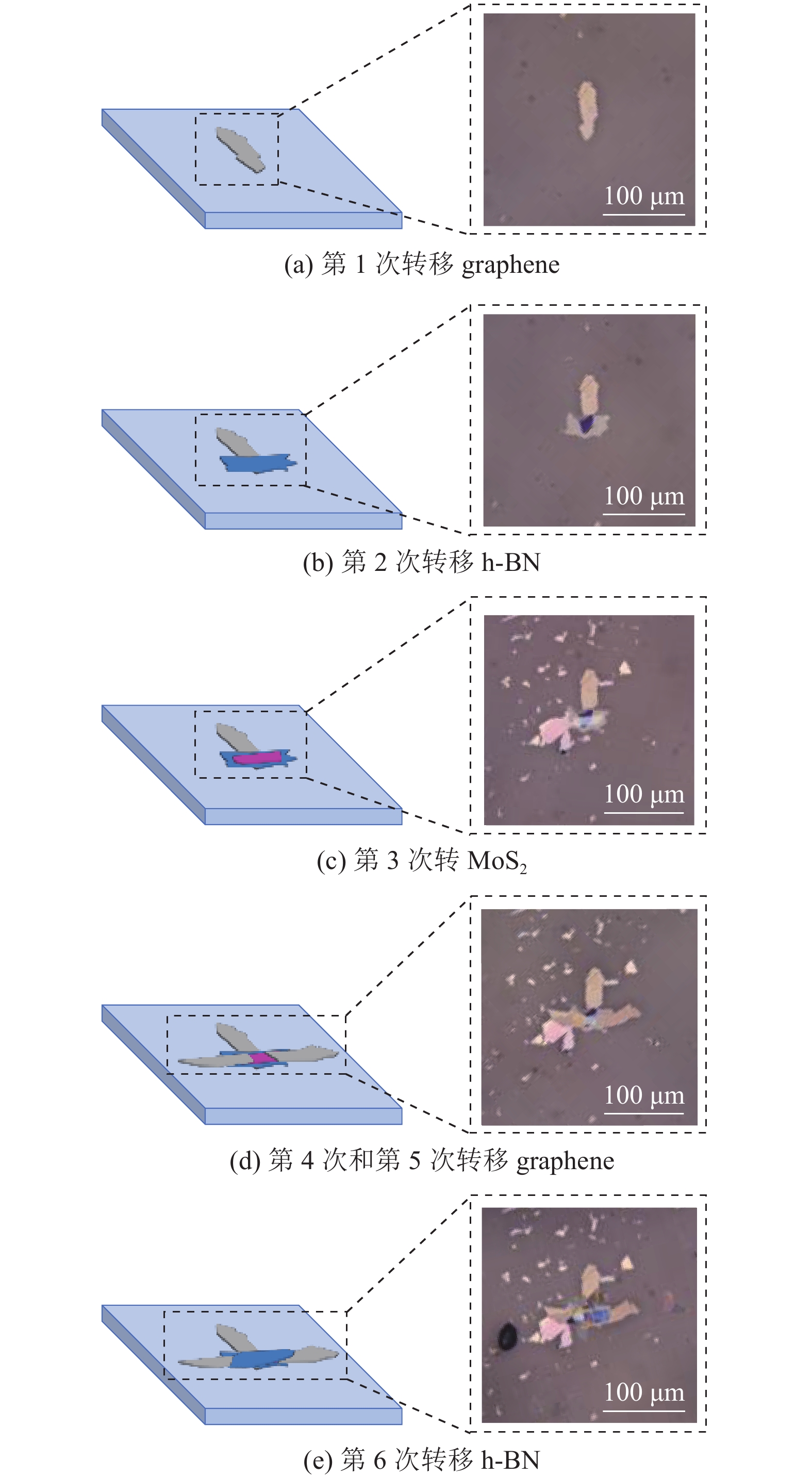
本文通过多次的干法转移,在柔性基底上制备出范德瓦尔斯异质结场效应晶体管,如图5所示。器件制备过程如下:第一次转移,在衬底上转移第一层graphene材料作为栅极,如图5a所示;第二次转移,在栅极的上方转移一层h-BN作为栅介质,如图5b所示;第三次转移,在h-BN的上方转移一层MoS2作为沟道材料,如图5c所示;第四次和第五次,在MoS2的两端转移graphene材料作为源极与漏极,如图5d所示;第六次,在器件的最上方转移一层h-BN最为保护层,保护器件,如图5e所示。
-
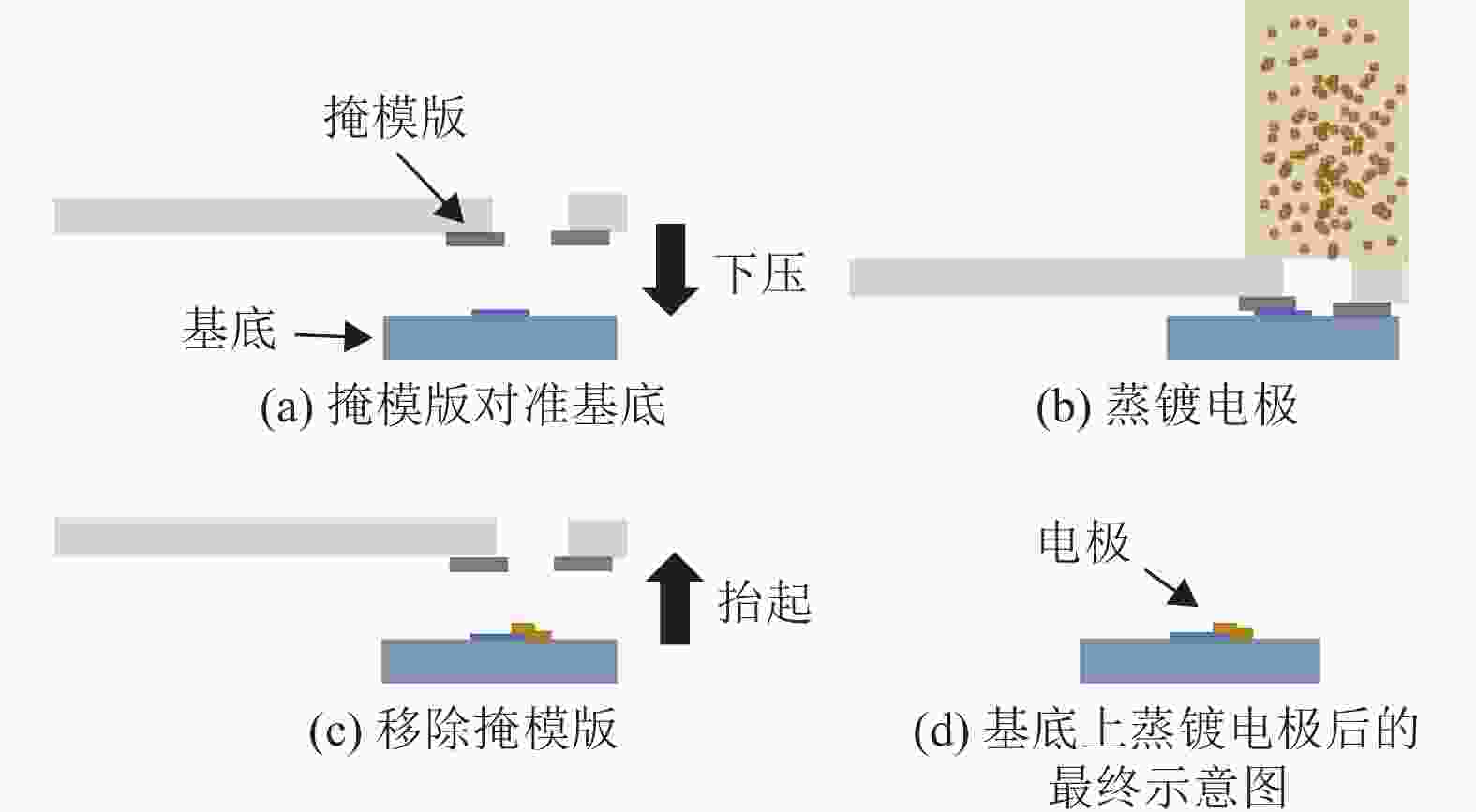
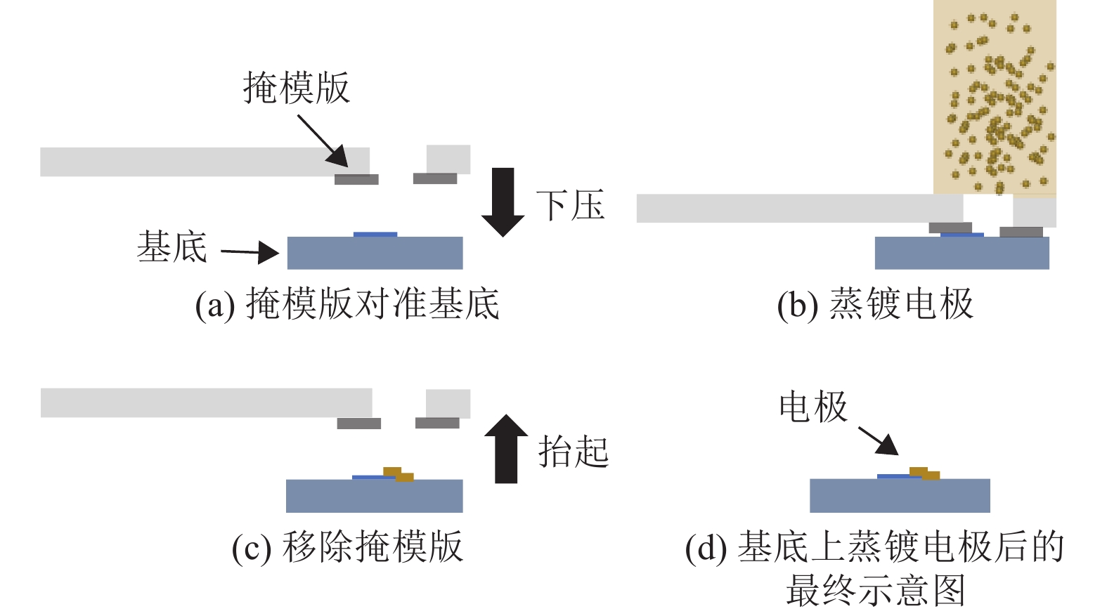
本文采用的基底为无金属电极的PET基底。因为没有预制电极,在干法转移与机械剥离时,对二维材料的面积大小,长度没有特别的限制,提高了器件制备的成功率。但同时,也需要研究者额外制备金属电极,从而与器件建立可靠的电学连接。本文采取的解决方法是使用真空蒸镀工艺,在器件的栅极,源极,漏极上淀积金电极[19-20]。
以为graphene蒸镀金属电极为例,如图6所示,首先,在光学显微镜中观察掩模版和graphene之间的相对位置,进行对准,同时缓慢下降掩模版直到完全与衬底贴合,如图6a所示;然后,将其放置在真空镀膜仪中,进行蒸镀,如图6b所示;最后,取下掩模版即可,如图6c所示。电极蒸镀完成后的结构,如图6d所示。该方法相对于采取光刻胶的方式,操作简单,不会污染材料。
-
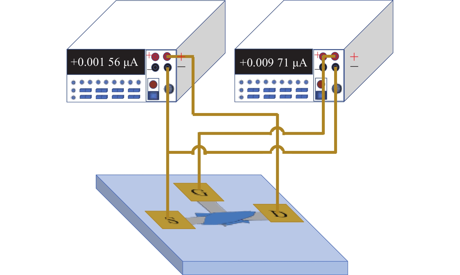
对范德瓦尔斯异质结场效应晶体管在柔性测试平台下进行电学连接,使用两台半导体参数分析仪连接器件如图7所示,两台半导体参数分析仪的低压端口连接在源端,一台半导体参数分析仪的高压端口连接栅极,另一台半导体参数分析仪的高压端口连接漏极。
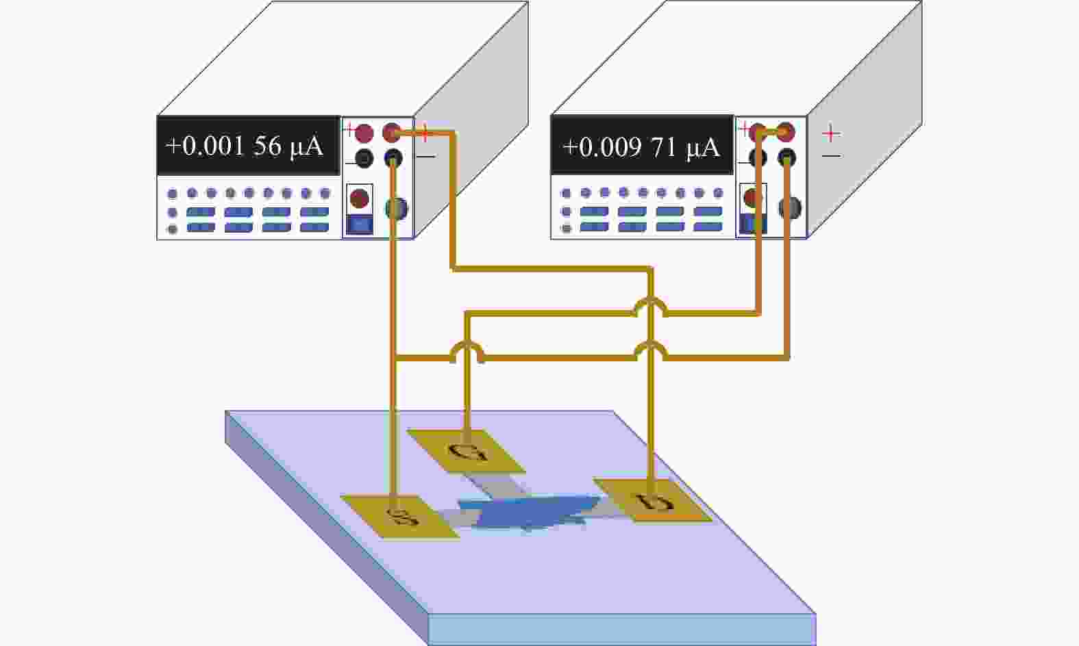
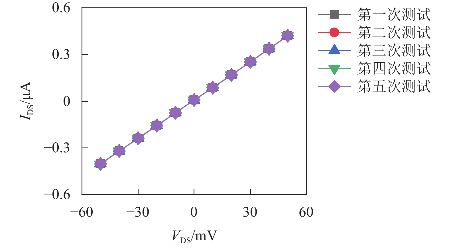
由于器件是多层二维材料堆叠形成,层与层之间电学接触对器件的正常工作至关重要,所以在进行器件的电学测试之前,本文先测试了器件能否正常导通。设置VGS=0 V,VDS为(−50 mV~50 mV),其测试数据如下图8,在栅压为零时,晶体管就退化为graphene\MoS2\graphene串联的电阻,从测试数据可以看出,器件电学接触良好,能够正常工作。
接下来,在测试平台上进行测试,测试主要分为两部分,一部分为器件机械性能的测试,如静态弯曲测试,或动态变化测试。另一部分为器件的电学的性能测试,如器件的输出特性,或器件的转移特性。所以两部分结合起来,一共具有4种不同的测试方案。
-
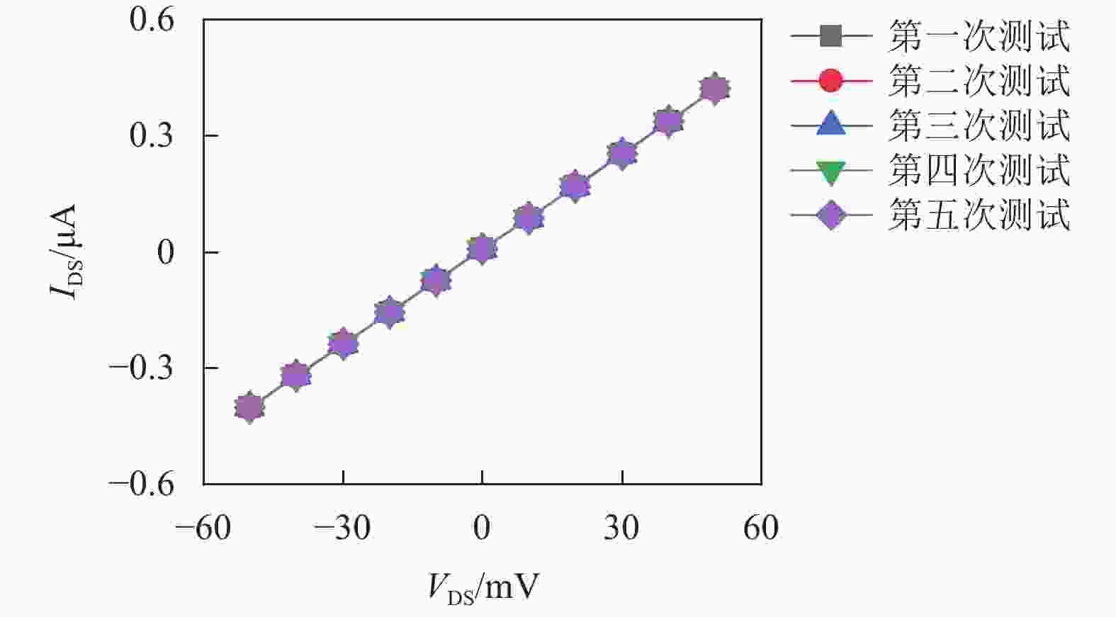
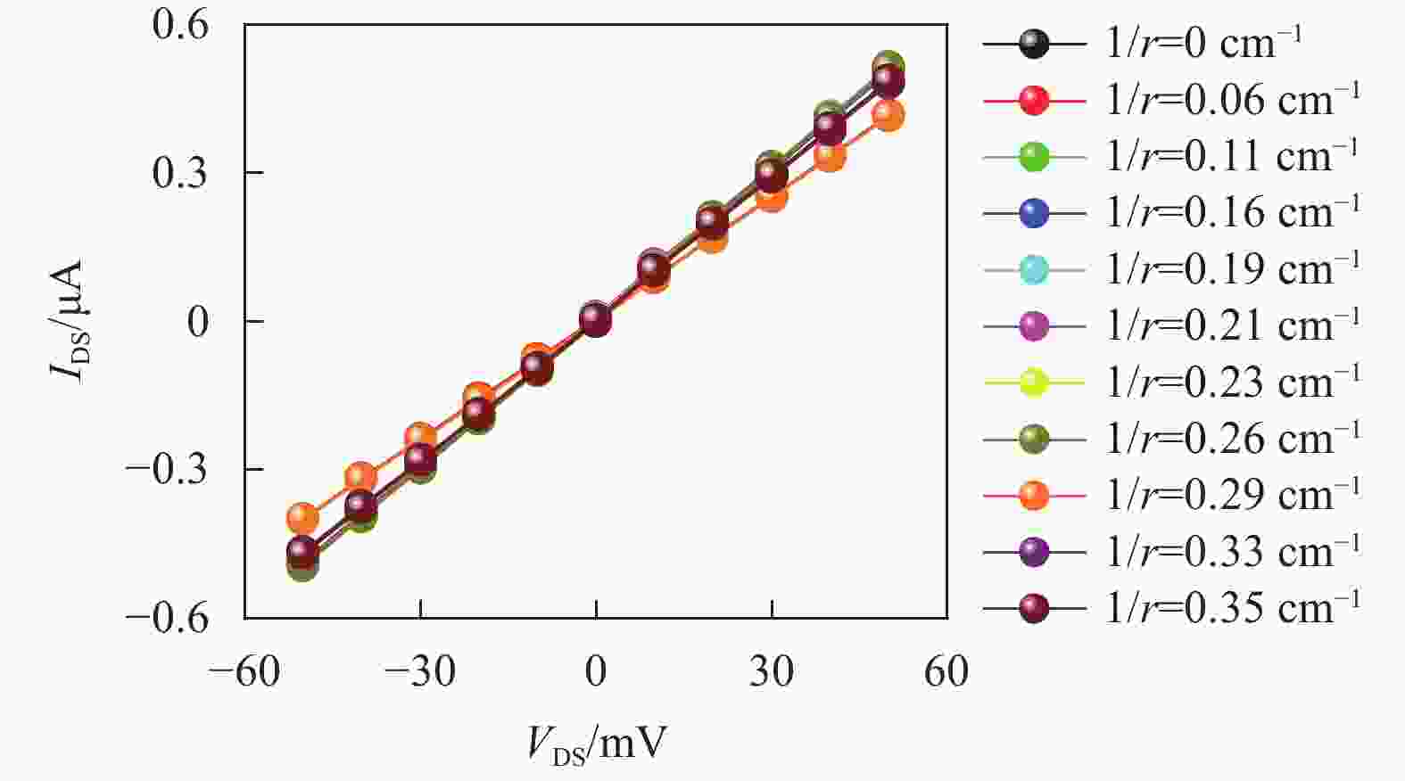
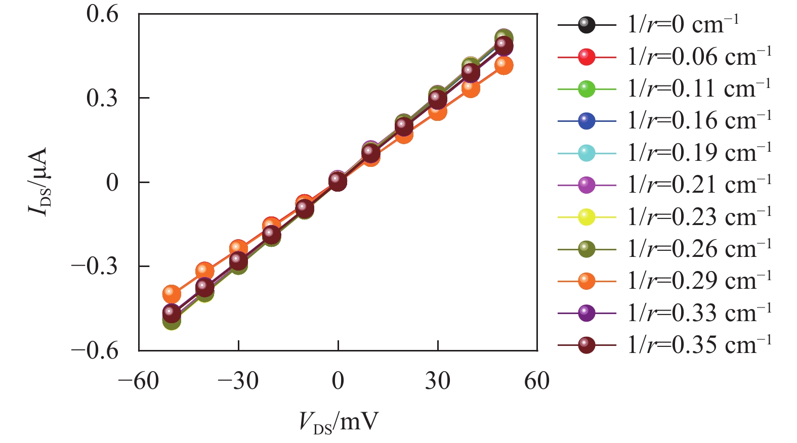
第一种测试方式是测试器件静态弯曲时的输出特性。设置VGS=1V,VDS(−50 mV~50 mV),在柔性测试平台进行静态测试,测试结果如图9所示。从图中可以发现,在静态测试条件下,器件的输出特性变化不明显,最大的变化率为25%,器件能够正常工作。
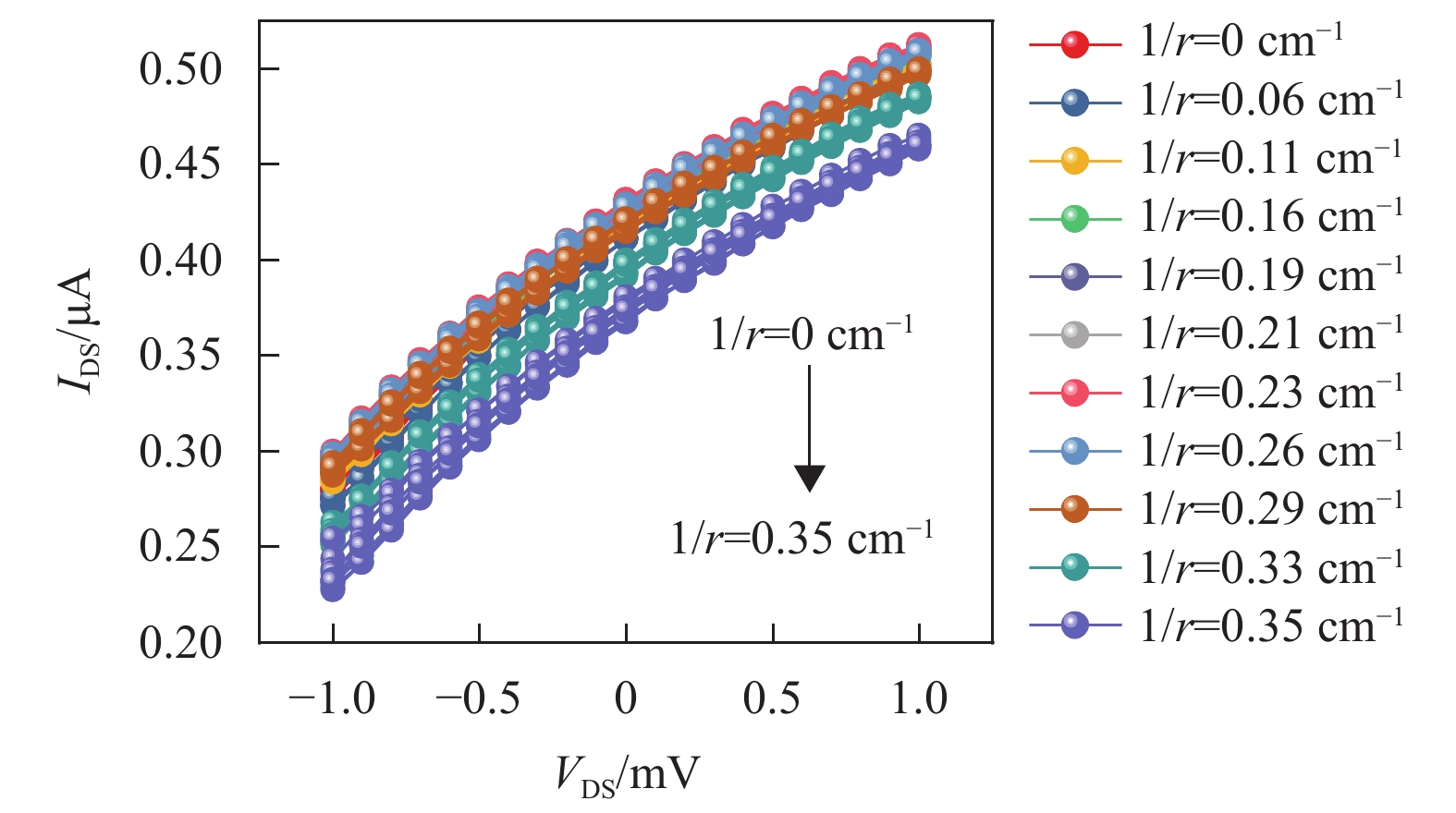
第二种测试方式是测试器件静态弯曲时的转移特性,设置VDS=0.05 V,VGS(−1 V~1 V),在柔性测试平台进行静态测试,完整的转移特性测试如图10所示。整体的变化趋势随着曲率的增加,器件的转移特性曲线往Y轴的负方向下降,如图中箭头所标识的方向。器件的阈值电压从−2.5 V(曲率为零时)下降到−1.2 V(曲率为0.35 cm−1时),器件的栅压调控能力下降。对于场效应晶体管的性能,更多的是希望,较小的栅压变化,能够引起较大的漏极电流的改变。而该柔性器件,在栅压改变1 V的时,器件的源漏电压改变了0.1 μA左右,栅压调控能力较弱。

-
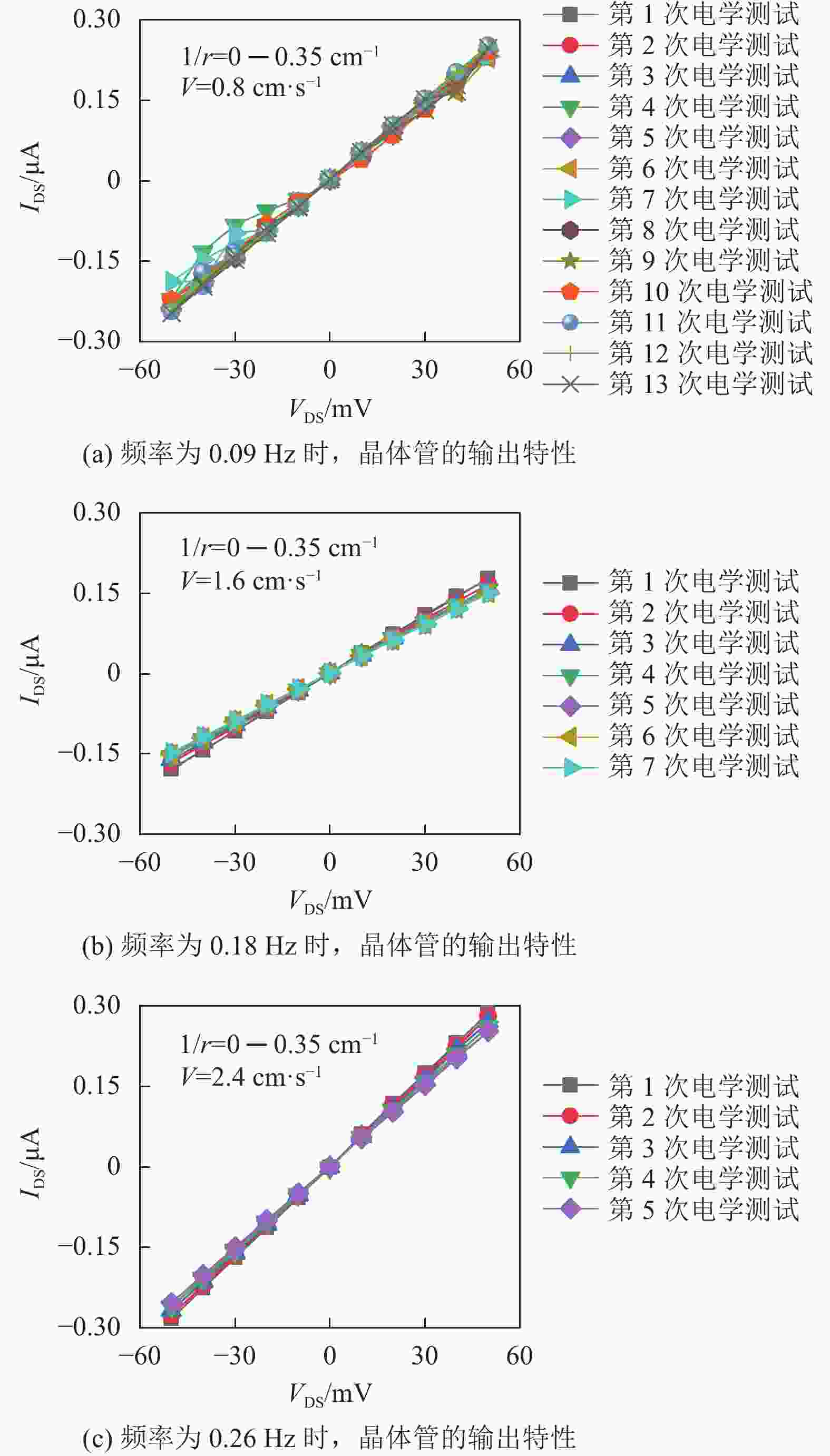
第3种测试方式是测试器件动态变化时的输出特性。设置VGS=1 V,VDS(−50 mV~50 mV),在柔性测试平台进行动态测试,测试数据如图11所示。从图11a中可以发现器件的输出特性相比于静态测试时,电流下降了0.3 μA,器件的性能下降,同时在多次的连续运动过程中,每次扫描的数据相对稳定,虽存在抖动现象,但没有持续发生,只是间隔出现。当位移台运动的速度设置为1.6 cm/s时,器件输出特性继续下降,电流下降0.15 μA,如图11b所示。而控制位移台运动的速度增加为2.4 cm/s,器件的输出特性反而变大了,相对于1.6 cm/s,电流提高了0.2 μA,如图11c所示。这有可能是由于材料堆叠造成的影响,导致在动态弯曲过程中,结构不稳定,使得器件的电学性能有较大变化。
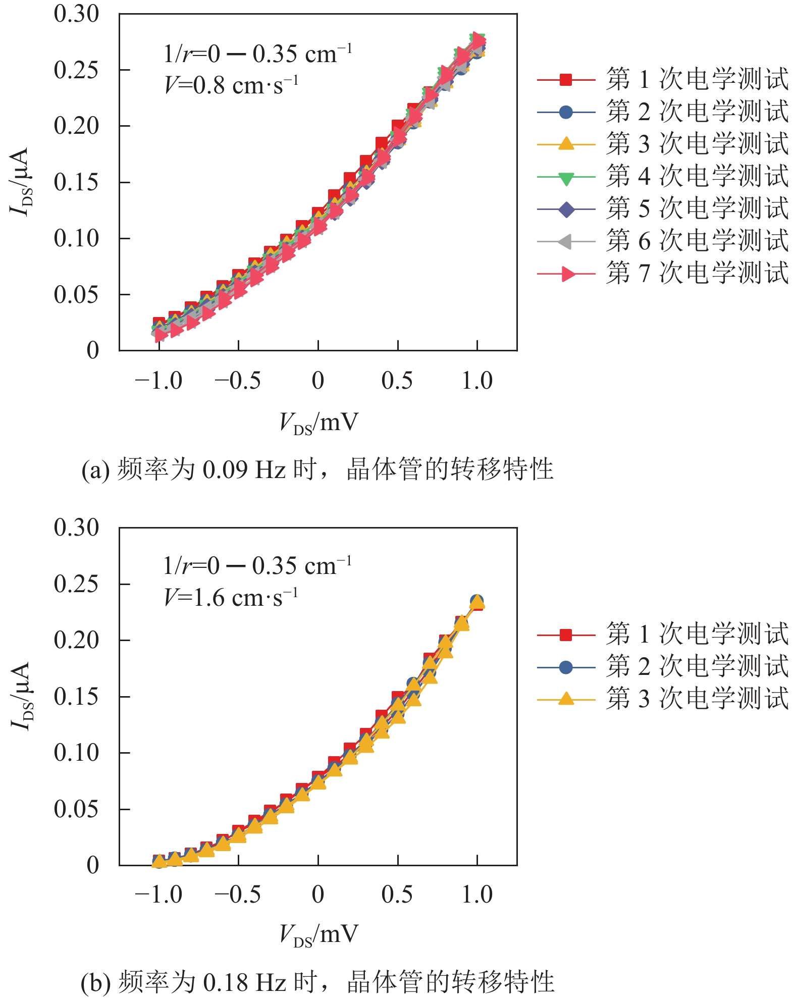
第四种测试测试方式是器件动态变化时的转移特性。设置VDS=0.05 V,VGS(−1 V~1 V),测试数据如所示。图9与图12对比发现,在位移台速度增加后,器件的转移特性曲线下降,阈值电压直接变为−1 V。此外,器件的最大电流与阈值电压都是明显下降。但是,在动态测试过程中,器件的转移特性变得更加陡峭,与静态测试对比,当器件的栅压从0 V变化至1 V,漏极电流变化了0.1 μA,而从图12a与12b中可以发现,器件的漏极电流变化了0.15 μA,器件的栅压调控能力提高了。与此同时,该器件在首次测试后出现了电阻大幅增加直至断路的情况,说明该器件电学性能虽然出现了一定改善,但仍然不够稳定。

从本文的测试数据可以发现,器件堆叠的层数越多、结构越复杂,就会导致测试结果无规律。部分可能的原因包括,材料之间依靠范德瓦尔斯力连接,当曲率较大时,衬底会有较大的拉伸应变,当应变大于范德瓦尔斯力时,有可能会造成层与层之间发生滑动。影响这一过程的因素有可能包括以下几点:1)机械剥离法制备的材料不够平整,厚度较厚;2)干法转移次数较多,每转移成功一次,就会与衬底之间形成台阶,后续材料的转移就不能与衬底贴合紧密。
通过以上分析,本文对后续的材料制备,器件结构提出以下改进方法:1)使用CVD工艺,制备尺寸较大,厚度较小的二硫化钼;2)不用石墨烯作电极,源漏电极通过蒸镀工艺直接制备在二硫化钼上;3)栅氧化层不使用六方氮化硼,改为Al2O3,用ITO作为栅极。改善后的器件结构有望避免上诉问题的发生,能够更好地研究范德瓦尔斯异质结场效应晶体管在柔性电子领域的应用前景。
-
静态测试时,位移台的运动速度较慢,不会损坏器件。动态测试时,位移台的设定速度增加后,器件在较短时间,经历了较大的应力变化,有可能会对器件特性造成潜在的影响。
为了减小二维材料发生位移、滑动的可能,可以在研究中采取如下方案:1)制备平整的薄层材料,避免材料与衬底形成较高的“台阶”;2)制备长度在100 ~ 150 μm的长条薄层二硫化钼,不使用石墨烯作为器件的源极和栅极,直接在二硫化钼长条的两端蒸镀金属,作为电极,排除石墨烯(源极/漏极)与二硫化钼(沟道)层与层之间发生位移滑动,这可以降低器件特性变化的几率。

-
当环境中的湿度较高的时候,会使得二维材料氧化变质,导致器件的性能下降。可以采取的解决方案包括:(1)器件的制备应在超净间中完成,控制环境中的湿度;(2)在器件结构制备完成后,转移一层二维材料作为保护层,保护晶体管的沟道材料。如本文图5中,最后一次转移h-BN作为保护层。
温度对器件的影响分为两部分,一部分为环境温度对器件的影响,另一部分为电流通过时,自身的焦耳热,对器件的影响。可以在超净间或真空恒温环境中测试器件,排除环境温度对器件的影响;PET衬底的散热能力较弱,当器件长时间通过较大的电流时,二维材料产生较大的焦耳热,导致损坏器件。可以采取的解决方案包括:1)源漏电压设置不能过大;2)不能进行长时间的电学测试,采取多次测量的方法,减小单次测试时间。
-
本文使用机械剥离法与干法转移,采取石墨烯作为电极、h-BN作为绝缘层、二硫化钼作为沟道材料,在柔性PET衬底上成功制备了范德瓦尔斯异质结场效应晶体管,研究了晶体管在静态与动态弯曲过程中的电学性能的变化。
本文晶体管的制备工艺简单,不需要复杂设备,具有更大的灵活性和可扩展性,能够高效地制造复杂的三维结构。此外,虽然二维材料层与层之间仅依靠范德瓦尔斯力连接,但是在静态测试时,器件曲率在(0 ~ 0.35 cm−1)之间,器件能够正常工作,电学性能只下降了25%。在动态测试时,我们发现电学测试结果呈现无规律变化,且晶体管容易损坏。表明使用机械剥离法与干法转移制备的柔性晶体管,在曲率变化率较大时,器件的结构不稳定。为了改善柔性晶体管的性能,本文从器件的结构设计、制备方法等方面入手,提出了未来可能有助于器件性能提升的优化建议。
Characterization of Electrical Properties of Flexible Transistors Based on van der Walls Heterostructure under Dynamic Strain Modulation
doi: 10.12178/1001-0548.2023104
- Received Date: 2023-04-21
- Accepted Date: 2023-05-19
- Rev Recd Date: 2023-05-29
-
Key words:
- two-dimensional material /
- field effect transistors /
- flexible devices /
- electrical characteristics
Abstract: Conventional electronic devices are mainly composed of inorganic semiconductor materials such as silicon-based and rigid polymer insulating substrate materials, which are the basis of existing electronic technology. Although the traditional electronic technology has been developed, but due to the limitations of the material, resulting in the field of flexible electronics, its application still exists in a certain limit. Two-dimensional materials have high crystallinity, near-perfect lattice structure, atomic-level thickness and high mechanical tensile strength, and exhibit excellent charge-transfer properties, making them promising for applications in the field of flexible electronics. In this paper, we combine the excellent mechanical properties of graphene, molybdenum disulfide and hexagonal boron nitride to prepare molybdenum disulfide-based field-effect transistors by mechanical exfoliation method with dry transfer. We test the flexible electrical properties of the devices using a flexible test platform built in-house. The test results show that the designed two-dimensional heterojunction transistor has only a small change in electrical properties under static test conditions; however, under dynamic test conditions, due to the too small van der Waals force between layers, the sliding or displacement between layers makes the electrical properties of the device change significantly.
| Citation: | CHEN Jianglong, WANG Zenghui. Characterization of Electrical Properties of Flexible Transistors Based on van der Walls Heterostructure under Dynamic Strain Modulation[J]. Journal of University of Electronic Science and Technology of China. doi: 10.12178/1001-0548.2023104

|


 DownLoad: