ISSN
ISSN 
| Citation: |
WANG Genwang, LI Lu, PAN Penghui, LI Baoxia. Current research and applications of 2.5D/3D integration technology for Multi-Chiplets[J]. Journal of University of Electronic Science and Technology of China. DOI: 10.12178/1001-0548.2024244

|
To address the demand for high-performance and high-integrity electronic chips in high-performance computing, artificial intelligence, and unmanned systems, advanced packaging and integration technologies, represented by 2.5D and 3D integration of multi-chiplets, not only overcome the challenges of decreased yield and increased costs in current integrated chips but also serve as a crucial means for integrating multiple types and functions of chiplets. This paper summarizes the current state of research and technological advancements in 2.5D and 3D integration of multi-chiplets, including 2.5D integration using large-scale interposers, 3D stacking integration with high density, and glass-based integration. Based on this review, the major development directions and key technical challenges of 2.5D and 3D integration are explored. Next, the applications of 2.5D and 3D integration in digital, optoelectronic, and microelectromechanical integrated chips and devices are reviewed. Furthermore, the development and application directions of multi-chiplet integration technologies are summarized, providing developmental insights for the realization of miniaturized, multifunctional, integrated chips and systems.
面对高性能计算机(high performance computer, HPC)、人工智能(artificial intelligence)、无人系统对电子芯片高性能、高集成度、多功能需求的不断提高,一体化集成芯片成为了未来电子系统发展的重要方向[1-2]。然而,单纯基于SOC(system on chip)技术的集成芯片在性能提升与多功能化的道路上面临着诸多问题,尤其是工艺制程继续缩小的难度呈现指数增大以及产品良率下降等。面对此瓶颈,台积电、英特尔等世界龙头企业提出了采用不同制程工艺分别制造不同芯粒,再在封装过程中对多个芯粒进行集成。该方法可有效降低集成芯片制造成本、提高产品良率,同时实现SOC集成与多功能化[3]。因此,除了“继续缩短制程”、“研制新原理器件”以外,基于多芯粒集成的先进封装技术成为了能够打破当前技术瓶颈又一条技术路线。并且由于继续缩短制程面临着技术、成本瓶颈,研制基于二维材料、宽禁带半导体等材料的新原理器件也离实际应用较远[4],因此多芯粒集成技术成为了快速提升芯片性能、实现多功能芯片产品化应用的重要手段。
目前,基于多芯粒的先进封装技术已经在英特尔、AMD、三星等企业的高端产品中成功应用,并且成为了世界各个机构、组织争相布局与发展的核心技术[5]。如美国国家标准与技术研究院、美国国家半导体技术中心等机构相继颁布一系列政策,重点发展多芯粒的2.5D集成、3D集成、光电共封等,并强调了多种制造、材料、功能芯粒的集成堆叠将是微电子技术发展的下一个浪潮。台积电、英特尔、三星、AMD等半导体龙头企业也在针对先进封装技术进行资源整合,建立发展联盟与技术平台,旨在争夺技术制高点并快速占领市场[6]。中国大陆方面,以长电科技、通富微电为代表的封装企业,以中国科学院、清华大学、北京大学、中国电子科技集团有限公司、中国航天科技集团有限公司为代表的研究机构均相继建立多项2.5D、3D集成技术能力,并成功研制了相关产品样件[7-8]。由此可见,多芯粒的2.5D、3D集成将是未来电子领域发展的重要方向。
本文以多芯粒的2.5D、3D集成技术为重点,总结当前世界先进集成技术方案与技术水平,分析不同技术优缺点与应用范围,归纳2.5D、3D集成技术发展方向与面临的技术难题。在此基础上,对基于2.5D、3D集成技术或相关技术的产品应用现状进行归纳与分析,探究该技术未来重点应用方向,包括数字芯片集成、高带宽内存(high band width memory, HBM)、互补金属氧化物半导体图像传感器(complementary-metal-oxide-semiconductor image sensor, CIS)、集成无源器件(integrated passive device, IPD)、微电子机械系统(micro-elector-mechanical system, MEMS)集成等。最后,对多芯粒的2.5D、3D集成技术面临的技术瓶颈与未来发展、应用方向进行总结,为后续实现高性能、多功能集成芯片提供研究方向参考。
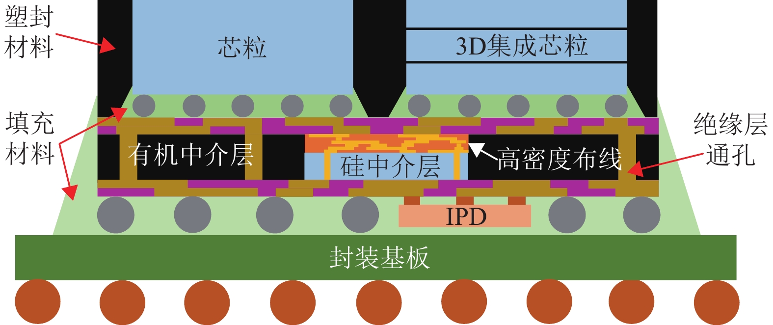
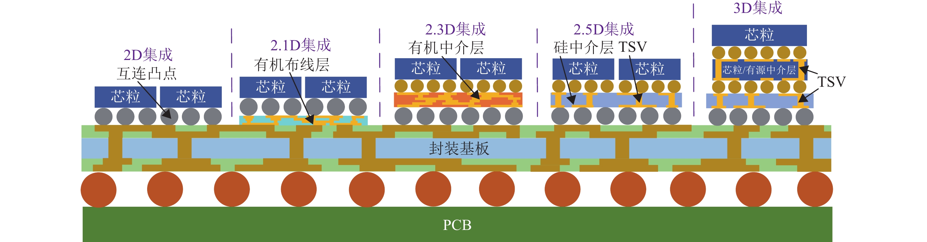
传统芯片封装技术主要是将单个芯片进行封装,然后通过封装基板或直接焊接至线路板(printed circuit board, PCB)上形成电学互连。先进封装技术则是针对多个芯片或芯粒进行集成与封装。按照芯粒间电学互连的空间维度,多芯粒集成可分为2D、2.1D、2.3D、2.5D、3D集成技术,如图1所示[9]。2D集成是将多个芯粒焊接至封装基板上,利封装基板上的电路实现芯粒之间水平方向上的电学互连。2.1D集成则是在芯粒与封装基板之间多了有机再布线层(re-distribution layer, RDL)。该层具有密度相对较高的互连线,并可嵌入硅基转接结构以满足高密度互连与较好的信号传输能力的需求。2.3D与2.5D技术则在芯粒与封装基底之间加入一层无源的中介层(interposer,或称转接板、转接基板等)。前者采用有机中介层,后者则是是使用基于硅通孔(through silicon via, TSV)的硅中介层。无源中介层的主要功能是实现多个芯粒在水平方向的高密度互连以及芯粒与封装基板在垂直方向上的互连。3D封装技术则是利用有源的TSV中介层,或直接在芯粒上制备TSV、互连微凸点与RDL等结构,通过等回流焊接、热压焊接、键合连接等方式实现有源芯粒在垂直方向上的堆叠集成。另外,随着异质异构芯片集成的需求的出现,2.5D、3D集成基于已不再局限于TSV技术,基于玻璃、陶瓷等材料的集成技术也在不断发展。在一些粗略分类中,2.1D、2.3D、2.5D技术也被统称为2.5D技术。本文将将采用该分类方法,对多芯粒的2.5D、3D集成技术现状进行总结与分析。
2.5D封装集成技术的有机布线层、有机中介层、TSV中介层上均可制备密度较高、性能优异的互连线,因此可以实现不同类型、不同制程的芯粒在水平方向上的高密度集成,不仅提高了集成芯片工艺良率,降低了集成芯片成本与能耗,也是实现多种功能芯粒集成的重要手段。目前,2.5D技术的典型代表有英特尔的嵌入式多芯片互连桥(embedded multi-die interconnect bridge, EMIB)技术、台积电的CoWoS(chip-on-wafer-on-substrate)技术、三星的I-Cube等。
EMIB技术是在封装基板的有机层中嵌入硅转接桥,提高了芯粒间的局部互连密度[10]。由于EMIB技术不仅可以实现高密度的I/O(每毫米的I/O数量达
CoWoS是将多个芯粒焊接至无源中介层上,使用中介层上的高密度布线进行集成互连。该技术可实现数量较多芯粒的高密度、低功耗集成。按照中介层材料不同,CoWoS技术可分为基于硅中介层的CoWoS-S、基于有机中介层的CoWoS-R以及局部硅中介层与全局有机中介层复合的CoWoS-L。CoWoS-S采用硅中介层、TSV以及微凸点互连等技术可实现动态随机存储器(dynamic random access memory, DRAM)、ARM(advance RISC machine)处理器、中央处理器(central processing unit, CPU)、HBM等多种芯粒的2.5D集成,且表现出了较好的可靠性[14]。目前,第五代CoWoS-S技术将中介层的尺寸已达
2.5D技术主要是实现多个芯粒在水平方向上的互连,更大尺寸的中介层意味着可以集成更多数量的芯粒。然而,为实现更大尺寸、更高性能的中介层,解决大尺寸集成中存在的结构翘曲、组件可靠性以及信号传输能力等问题成为了需要攻克的技术难点。如三星将ASIC、HBM等芯粒进行2.5D集成与底部填充后,对整个集成芯片进行了塑封,再焊接至具有加强环结构的封装基板上[20]。塑封材料与加强环结构能够有效地缓解大尺寸中介层中的翘曲问题,使翘曲减小至50 um。并且该结构也提高了组件可靠性,可承受−55°C~125°C的温度循环[21]。台积电在第五代CoWoS-S中加入了集成电容以提高电源完整性,并且采用新型的微凸点结构与TSV结构,减小了电阻、插入损耗与回波损耗,同时研制了一种热界面材料,降低了集成芯片的热阻抗[15]。台积电也开发了集成了IPD与硅转接结构的CoWoS-R+方案,进一步降低了信号传输中的损耗[22]。类似地,CoWoS-L中也采用了集成电容对信号传输能力进行了优化,并且全局有机中介层也有利于缓解大尺寸集成中的翘曲问题[18]。因此,随着集成芯粒数量的增加, 2.5D集成技术在大尺寸中介层的结构可靠性、电学特性等方面仍面临诸多亟待攻克的技术难点。
在面临2.5D中介层尺寸增大、信号传输能力提高存在瓶颈时,能够在垂直方向进行芯粒堆叠集成的3D封装集成技术成为了进一步提高集成密度的重要手段。3D集成的关键是需要在有源芯粒或中介层上制造互连通孔,然后对芯粒进行堆叠与垂直电互连。目前,最先进的3D集成技术有英特尔的Foveros、台积电的SoIC、AMD的3D V-chache、三星的X-Cube等。
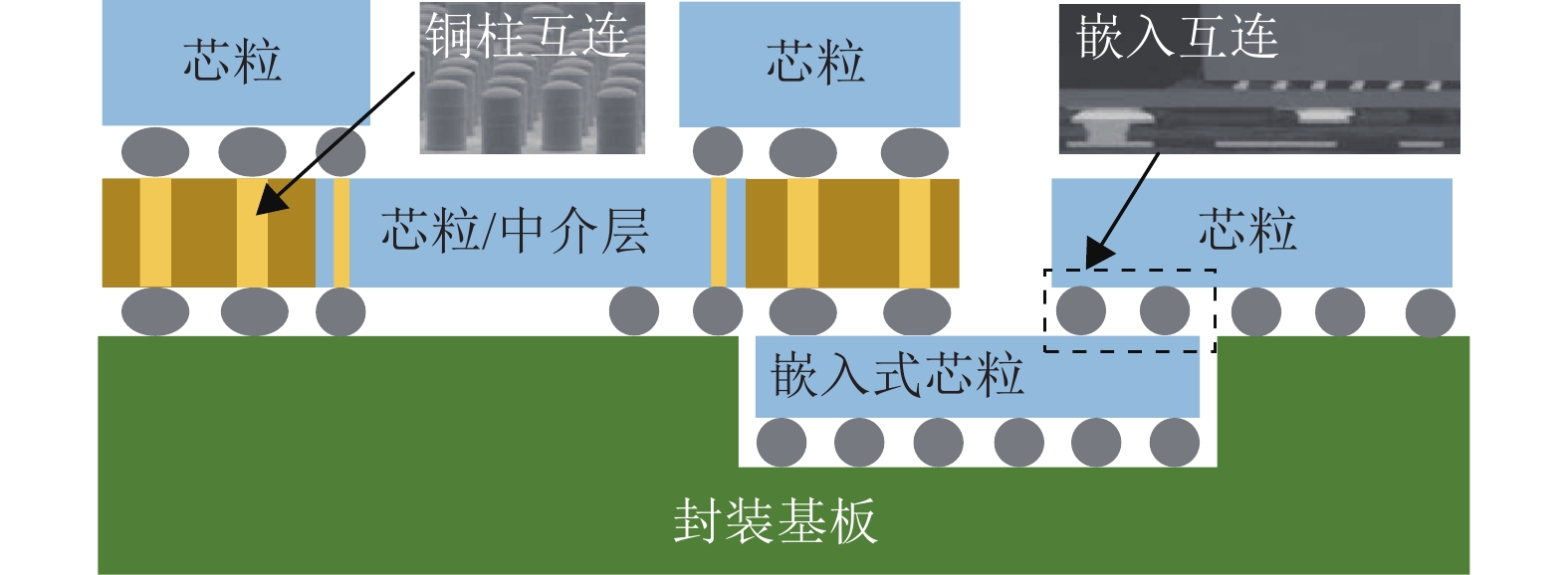
Foveros技术主要利用TSV、RDL以及层间微凸点实现有源芯片的堆叠互连,更适用于高集成密度、对内存带宽要求更高的产品。目前,Foveros的互连节距可到36-50 μm,有望实现较高密度的集成,同时集成芯片具有较好的可靠性与信号传输能力[23, 24]。然而,TSV的大量使用会导致传输损耗增加、带宽减小,互连凸点的尺寸难以继续缩小也限制了集成密度的提高。因此,英特尔提出了Foveros Omni与Foveros Direct技术。Foveros Omni采用一种全方向层间互连技术(omni directional interconnect,ODI),如图3所示[25]。相比于只能进行单一方向互连的TSV硅中介层,ODI利用铜柱连接结构或嵌入式芯粒代替TSV,可以实现芯片之间的连接以及顶部芯片、底部芯片分别与封装基板之间的连接。ODI使得集成芯片在整体尺寸不增加的情况下避免过长的布线,并能够保持高带宽传输,且有利于降低工艺成本。Foveros Direct则是采用混合键合(hybrid bonding, HB)技术实现芯粒层间堆叠互连,由于HB是一种无凸点的垂直互连,可使互连节距小至3 μm,并且具有较小的互连电阻与寄生电容[26]。该技术是未来实现高密度集成的重要手段。英特尔基于HB技术还提出一种准单片系统(quasi-monolithic chips, QMC)。其目的是打破芯片制造与封装之间的壁垒,使晶圆厂就可以完成整个芯片制造与封装集成过程[27]。但QMC技术增加了SiO2绝缘层的制备、磨平以及制孔等工艺,易出现绝缘层崩边、芯片边角处应力集中、晶圆翘曲等问题。
台积电的SoIC技术也采用TSV、HB等技术,以实现10 μm以下互连间距的高密度3D集成,并具有较高的带宽、较低的功耗以及优异的电源与信号完整性。研究表明,与其他封装技术相比,SoIC可以将互连密度提高16倍,带宽密度提高191倍,能耗降低95 %[28]。为进一步提高互连密度,第四代SoIC技术的互连节距可以小至3 μm,第五代技术有望减小至2 μm[29]。SoIC技术关键指标的提升如表1所示。另外,台积电也提出了更高互连密度的SoIC-UHD技术,有望将互连节距降低至0.9 μm[30]。
| 技术 | 第一代 | 第二代 | 第三代 | 第四代 | 第五代 |
| 互连节距(μm) | 9 μm | 6 μm | 4.5 μm | 3 μm | 2 μm |
| 带宽密度提升 | 1.0x | 2.0x | 3.4x | 6.1x | 11.5x |
| 能耗效率提升 | 1.0x | 1.0x | 1.2x | 1.3x | 1.4x |
 DownLoad:
CSV
DownLoad:
CSV
类似地,AMD的3D V-Chache技术以及三星的X-Cube技术也是基于TSV、凸点互连或HB技术的3D集成技术,并也朝向低节距、低功耗互连发展[31]。
综上可知,降低互连节距是3D集成技术目前发展的重点方向。HB技术的出现与应用为高密度互连提供了技术支持,是未来主流互连技术发展方向。然而,HB不仅对工艺环境、设备能力方面提出了较高的需求,同时低节距的互连还会导致信号传输干扰、电流拥挤等问题[26]。因此,基于HB的3D集成技术在结构设计、电源信号完整性方面还需要进一步提升。另外,与2.5D集成类似,TSV的出现也会引起阻抗大、发热累积等问题。ODI技术就是采用铜柱等互连结构,减少了TSV的数量,使得组件的电学性能得到改善[25]。因此,在不断提高互连密度的同时,解决低互连节距与高性能电学特性之间的矛盾,是未来3.5D集成技术研究的重点。
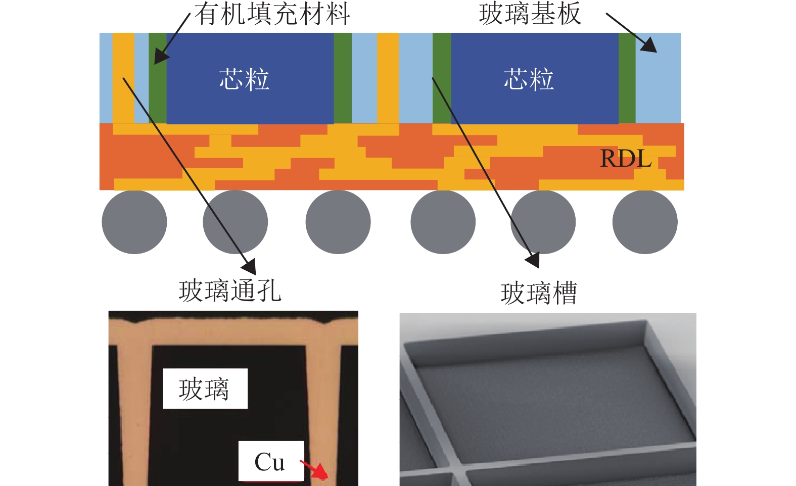
在2.5D、3D集成技术不断发展的同时,硅基集成技术在材料丰富程度、工艺成本、功能多样性等方面的先天短板也日益明显。玻璃、陶瓷等材料成为了进一步丰富封装结构、实现多功能芯片集成的关键。佐治亚理工学院提出了采用玻璃中介层可有效减小信号传输损耗、降低成本,同时通过调控玻璃的热膨胀系数等特性可以解决硅芯粒与基板之间直接互连的可靠性问题,降低封装成本[32]。为此,佐治亚理工采用激光烧蚀的方法在玻璃上制备了直径为15 μm的玻璃通孔(through glass via, TGV),其插入损耗可低至0.15 dB[33]。进一步地,康宁公司在玻璃上制备了TGV与RDL,获得了高性能的玻璃中介层,证实了玻璃中介层的信号损耗小于硅中介层[34]。在玻璃中介层可靠性方面,Unimicron公司制备了尺寸为21 mm×14 mm、厚度为0.1 mm的2.5D玻璃中介层[35]。并且该中介层在进行了172次−55℃~125℃的温度循环后,性能无明显变化。Dai Nippon Printing公司则制备了具有线宽/间距约为2 μm的玻璃中介层。该基板可承受
陶瓷材料具有耐高温、耐腐蚀、气密性好、成本低等特点,是封装技术中必不可少的关键材料。由于陶瓷材料具有可调的膨胀系数,因此陶瓷材料多用于封装基板中,以提高芯片、封装基板、PCB的整体可靠性[39]。另一方面,随着高性能、一体化集成芯片的需求不多增加,散热问题成为了产品可靠性的关键。高导热率的陶瓷材料为高性能散热提供了技术手段[40]。然而,受限于陶瓷通孔(through ceramic via, TCV)制备精度、再布线密度等,陶瓷基板难以实现芯粒间的高密度互连,在2.5D、3D集成中的应用较为局限。直径100 μm以下的TCV制备成为了未来陶瓷基2.5D、3D集成的关键难题[41]。
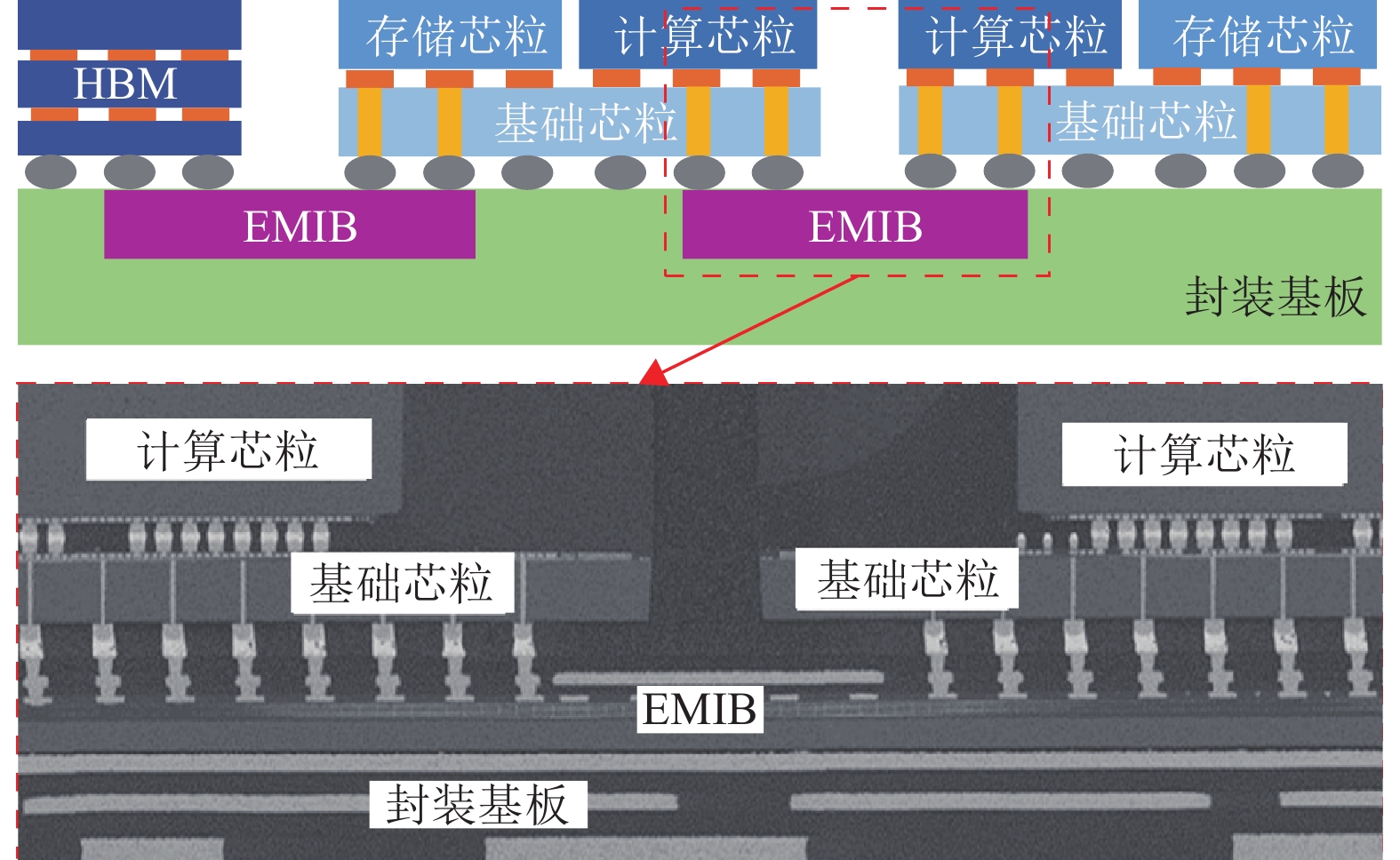
随着多芯片集成技术的不断发展,多种数字芯粒的2.5D、3D集成逐渐应用于商业化芯片与电子系统中。EMIB技术已应用于英特尔的Stratix 10系列、AgileX系列的现场可编程逻辑门阵列(field programmable gate array, FPGA)芯片产品,实现了基于2.5D无源基板的芯粒之间、芯粒与收发器的互连[42-43]。相比于EMIB,CoWoS以更高集成密度、更低功耗、更高算力的优势,在NVIDIA的高端GPU中更具有巨大的应用潜力,有望满足未来AI、HPC技术的需求[44]。LakeField处理器最早采用了3D集成Foveros技术,实现了来自10 nm制程工艺与22 nm FinFET工艺的CPU、GPU、IPU以及其他基础芯粒的集成,集成后的尺寸小至12 mm×12 mm×1 mm[45]。新一代的Meteor Lake处理器以及后续的Arrow Lake、Lunar Lake等产品都将继续采用Foveros集成技术[46]。英特尔的Ponte Vecchio系列GPU则采用了结合EMIB、Foveros的Co-EMIB技术,将来自5种不同制程工艺的47颗逻辑芯片、SRAM、HBM等芯粒进行了2.5D、3D集成,如图5所示。其中,采用了11个EMIB结构实现了多种芯粒的2.5D集成,采用Foveros将存储芯片进行了3D堆叠[11]。AMD的在多款EPYC、RYZEN处理器运用3D V-chache集成技术,将L3缓存提高至96 MB[47-48]。因此,多种2.5D、3D集成技术已成功在商业化产品中得到应用,为芯片微型化、功能多样化与性能提升提供了技术手段。
2013年,AMD联合SK海力士推出了基于3D集成技术的多层堆叠的高带宽DRAM——HBM,并且定义了JESD235行业标准。随后,SK海力士报道了4层DRAM堆叠的HBM。该堆叠内存的带宽为128 GB/s,内存容量为1 GB[49]。HBM层间连接方式采用TSV与微凸点回流焊接技术,单个TSV的阻抗可降低至0.1 Ω。在此基础上,SK海力士建立了TSV修复技术,并对该产品的带宽等性能、测试方法进行了提升[50]。2016年,三星报道了第二代产品HBM2。其堆叠层数为8层,单个引脚速率为2.4 Gb/s,内存容量为8 GB,电压为1.2 V,带宽提升至314 GB/s,并通过改进刷新方案、TSV布局等进一步提高了HBM的能量效率 [51]。HBM2内存堆栈不仅比HBM1更快,而且容量更大。2020年,JESD235C标准规定了新一代HBM2E的指标。三星与海力士都推出了相关产品,实现了8个的芯片堆叠,内存为16 GB,整体带宽可达640 GB/s,且单个引脚速率可达5.0 Gb/s,电压降低至1.1 V[52-53]。
2022年,JEDEC正式发布HBM3标准JESD238。根据此标准,SK海力士的HBM3产品首次实现了垂直堆叠12个DRAM芯片,芯片容量为16 GB,单个引脚速率为7.0 Gb/s,最大带宽为896 GB/s,且电压降低至1V,功耗降低15 %[54]。三星也报道了带宽为
DownLoad:
CSV
封装集成中的TSV工艺为实现背面辐照(back-illuminated,BI)CIS与数字芯片的三维集成提供了基础。Sony公司推出了一款双层堆叠的BI-CIS,将感光芯片堆叠在逻辑芯片、模数转换(analog-to-digital converters,ADC)芯粒上,并采用TSV实现双层芯片的电学互连[60]。在此基础上,Sony又提出了具有双单元ADC的BI-CIS产品,使产品的刷新速率提高至120 fps,且分辨率达16M像素[61]。在此双层BI-CIS结构中,层间的电学连接是在感光区域的侧边制备TSV。虽然TSV便于层间互连,但也会占用一部分芯片尺寸。为进一步减小芯片的整体尺寸,Sony在芯片背面进行布线,并用HB技术将连接线路置于感光区域下方,不仅降低了成本,也缩短了连接线路的长度[62]。在提高互连密度的同时,基于HB的CIS仍能保持较好的电学性能以及图像处理能力。类似地,三星也在CIS中引入了HB技术,并将互连节距从6 μm减小至1 μm,进一步提高了互连密度,使高分辨CIS成为可能[63, 64]。
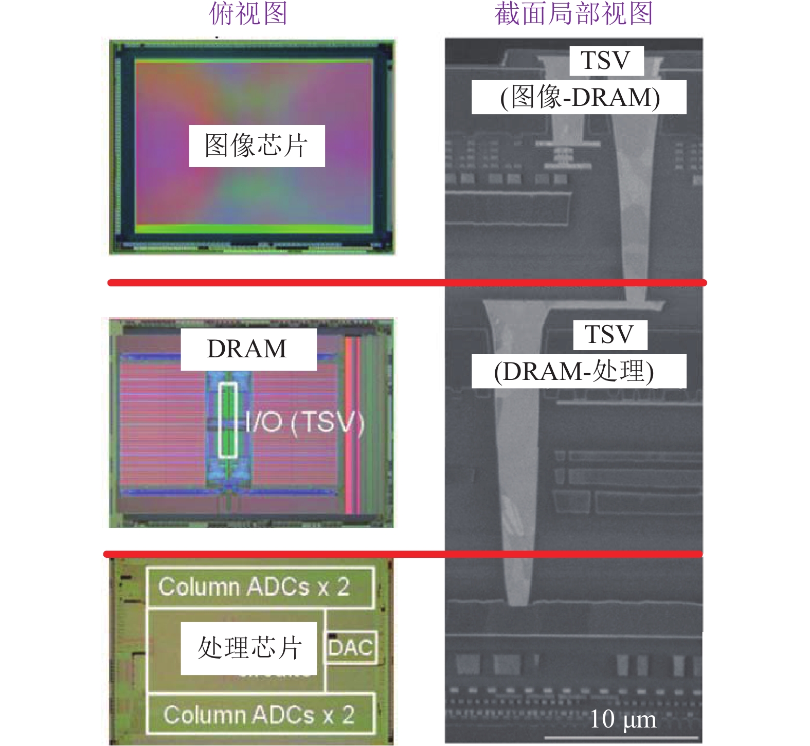
双层BI-CIS的读写速度受限于逻辑芯片的输出,使得高速摄像下出现图像扭曲现象,难以满足高速摄像发展的需求。为解决这一问题, Sony在像素芯片与逻辑芯片之间加入DRAM,实现了三层(图像传感器、DRAM、数据处理芯片)堆叠的CIS产品。其中,DRAM用于暂时储存来自像素芯片的数据,以实现高速成像[65]。三层堆叠的层内TSV的最小直径为2.5 μm,节距为6.3 μm。单个芯片的TSV数量可达
随着芯粒集成技术的发展,2.5D、3D集成电路对电源、信号稳定性提出了更高的要求。面对电压下降、阻抗失配、噪声纹波等问题,IPD在集成电路去耦、滤波以及信号处理等方面的重要性愈发凸显,对于提高集成电路的性能和可靠性起到关键作用。2.5D、3D集成技术中的深硅刻蚀、再布线制备等也成为了实现IPD微型化的关键工艺技术。
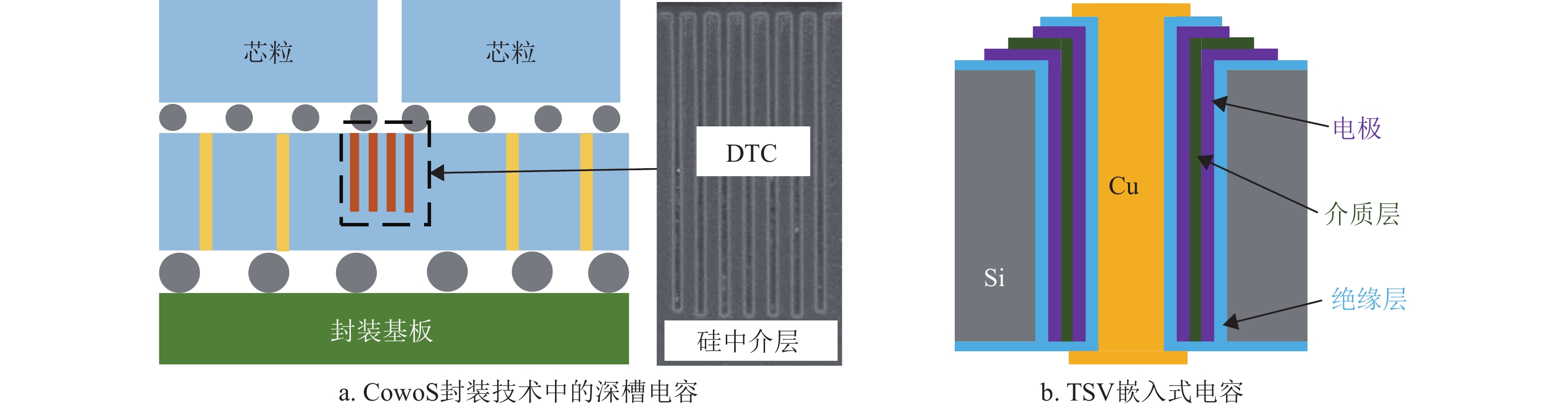
集成电容是2.5D、3D封装IPD的典型代表。2014年,台积电在CoWoS封装方案的硅中介层中集成了“金属-绝缘层-金属”结构的平面电容,电容密度达到17.2 nF/mm2[68]。然而,受芯片上可用面积的限制,平面电容的电容密度难以继续提高。2019年,台积电在CoWoS中介层上制备了深槽结构,利用在三维深槽结构表面制备薄膜电容,获得了三维深槽电容(deep trench capacitor,DTC),如图7(a)所示[69]。三维结构的出现使得在保持硅中介层上占用面积不变的同时,增加了电容尺寸,使得单个DTC的电容密度可达340 nF/mm2。随后,台积电在HBM与其他芯粒的集成中也加入了DTC,有效地降低了信号传输阻抗、噪声等[15, 70]。2023年,台积电在CoWoS-L中集成的DTC的电容密度可达
除深槽结构的三维电容,其他结构形式的电容也在研究中。为进一步增加DTC的电容密度,日本东北大学在褶皱结构的硅表面上制备了基于氮化硅的3D电容,进一步利用褶皱结构增加了电容尺寸与电容密度[72]。三星提出了一种集成堆叠电容方案,进一步减小3D电容的尺寸,并减小信号传输阻抗[73]。清华大学通过仿真研究了基于高密度微小尺寸柱状结构的3D电容,并证明了六边形柱状结构3D电容的电容密度可达
集成电感可分为位于基底上或嵌入基底内的2D电感、3D电感[79]。其中,利用TSV/TGV与再布线互连形成的3D螺旋电感表现出了较高的电感密度与品质因素[80, 81]。3D集成电感的主要研究方向是在有限空间内增加线圈截面积、提高绕组圈数、增加磁芯结构,以提升电感密度、工作频率等性能。另外,基于电阻、电容、电感也可实现其他无源器件电路。例如,英特尔采用集成电感构建了集成电压调节器(integrated voltage regulator,IVR),将转换效率提高至91.5 %[82]。中科院在玻璃基板填埋了射频收发芯片,通过RDL构建了集成转换器[83]。Zhang等人借助玻璃基板以及TGV技术,研制了带通滤波器,其插入损耗为−2.1 dB,回波损耗为−10 dB[84]。基于TSV/TGV技术,功率分配器、巴伦、射频耦合器等无源电路也有望实现小型化[85-87]。
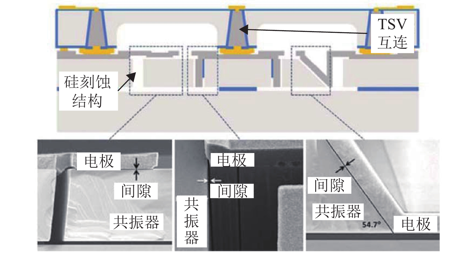
MEMS器件在传感领域、惯性领域等有着广泛应用。随着对多功能芯片集成需求的日益增加,数据处理芯片与MEMS的集成也成为了2.5D、3D集成技术的又一重要应用。多种芯片与MEMS的集成,不仅缩小了整个传感系统的尺寸,同时使其性能增强、功能多样化。例如,柏林工程应用技术大学提出了一种贴装于飞机机翼底部的压力传感器[88]。该传感器主要基于TSV、倒装焊接技术将MEMS结构与ASIC、FPGA等芯片的集成互连,可用于飞机飞行过程中的气流检测。挪威国防研究院研制了一种用于超加速的数据记录器,主要采用2.5D集成技术将微控制器、闪存芯片、MEMS加速器、去耦电容等组件集成在TSV硅中介层上,再将其与电源、滤波器等其他元器件相集成[89]。此数据记录仪的整体尺寸小于9 mm,可用于12.7 mm的发射物上以记录其加速度,最大可测试加速度可达
以2.5D、3D集成为主的先进封装技术经历了十多年的发展,出现了以硅基器件为主要对象的多种封装集成技术。在2.5D集成技术,硅中介层集成技术在高密度布线与集成中占据优势,有机中介层表现出了较低的成本与较好的传输性能,全局有机中介层与局部硅转接互连在一定程度上有效地结合了二者的优势,同时有望实现更大尺寸的集成。2.5D集成技术未来仍是面向大尺寸、多芯粒的异质集成发展,亟待攻克的技术问题包括:(1)继续优化TSV结构与位置、提高RDL布线密度,进一步提升集成密度;(2)实现更大尺寸中介层以集成更多数量的芯粒,重点解决大尺寸基板引起的翘曲、可靠性问题;(3)优化中介层互连网络的电学性能,降低集成芯片功耗,提高信号、电源完整性,包括集成多类型的无源器件,并且促进集成芯片在高频信号领域中的应用。对于3D集成技术,目前的主要发展方向包括两点:1)基于混合键合及相关工艺技术,将互连节距降低至几微米甚至是亚微米,大幅度提高集成密度与能耗效率,实现更高密度的多层堆叠互连;2)解决高密度3D堆叠互连中的阻抗大、发热等问题,进一步优化互连结构,以提高堆叠芯片的整体性能。
除硅基集成技术以外,以玻璃、陶瓷等材料的2.5D、3D集成技术成为了弥补硅基集成先天短板、丰富集成材料及工艺库的重要手段。尤其是玻璃集成技术具有材料特性可调、成本低、高频应用潜力大等特点,同时也是实现无源器件集成、光电共封技术的重要手段。然而,受限于TGV、TCV在孔径尺寸、孔形貌控制等方面目前还难以与TSV匹敌,相关RDL制备、晶圆减薄、电镀填充等工艺也有待进一步提升,玻璃、陶瓷材料的应用目前暂时还停留在封装基板层级,在2.5D、3D集成中介层中的研究还有待进一步加强。
多芯粒2.5D、3D集成技术已经在数字、光电、MEMS芯片集成中得到了广泛应用。尤其是在FPGA、CUP、GPU、HBM等数字芯粒的集成方面,已经进入产品化阶段。其中,基于3D集成技术的HBM成为了SK海力士、三星、美光等国际领头企业的技术角逐点,多层DRAM芯粒的堆叠成为了实现大容量、高带宽、小尺寸的存储芯片的重要技术手段。HBM未来将继续实现更多层数、更低能耗、更高容量、更高带宽的技术目标发展。但以HB为代表的高密度互连技术在HBM中的应用还需要进一步研究。CIS的集成对微米级互连节距的需求最为迫切,较低的互连节距以及多种存储、处理芯片的集成是提高CIS分辨率与刷新率的关键。CIS未来仍会向更多堆叠层数、更小互连节距发展。除了工艺技术上的提升,也迫切需要优化互连架构,改善光电信号的处理能力。IPD不仅可以用于2.5D、3D集成中电学信号传输与处理能力的提升,也是提高集成芯片在高频信号领域应用的关键。三维电容是IPD技术的典型代表,并已经在CoWoS、SoIC等集成方案中得到应用,未来将朝向更高电容密度与耐压性、更小ESR与阻抗等目标发展。电感、滤波器等其他无源器件也再朝向更小尺寸、更高性能发展。MEMS与数字芯片的堆叠集成也是2.5D、3D集成技术的重要应用方向,三维互连为实现更小尺寸、更高性能的MEMS器件提供了技术手段。然而MEMS器件对整个芯片的应力分布、温度控制的要求较高,如何平衡高密度集成与器件性能需求、解决TSV及互连结构对传感结构的影响是MEMS集成技术未来需要攻克的重点方向。
本文针对2.5D、3D封装集成技术,总结了以台积电、英特尔等龙头半导体企业的先进集成方案与技术水平,归纳了目前以大尺寸2.5D中介层技术、低互连节距3D堆叠互连技术为代表的主要技术发展方向,分析了当前技术发展仍对结构与功能可靠性、信号传输与处理能力以及互连工艺能力等技术提升有着迫切需求。同时,玻璃、陶瓷等材料在封装集成技术的应用与发展也有望进一步弥补当前硅基集成技术的不足。在此基础上,进一步对2.5D、3D封装集成技术在CUP、GPU、HBM等数字芯片集成、CIS芯片集成、面向封装集成的IPD、MEMS器件集成方面的应用进行总结分析。2.5D、3D封装集成技术不仅在实现芯片与器件微型化、高性能化带来了技术提升,同时为多种功能异质芯片的集成以及多种类型信号的处理提供了技术手段,促进了未来多功能一体化芯片的实现。本文最后对多芯粒2.5D、3D集成技术的发展与应用方向进行了总结,归纳了技术发展仍面临的重大挑战,为后续集成技术的发展提供指导思路。
| [1] |
WANG Z Y, SUN J B, GOKSOY A, et al. Exploiting 2.5D/3D heterogeneous integration for AI computing[C]//Proceedings of the 29th Asia and South Pacific Design Automation Conference. New York: IEEE, 2024: 758-764.
|
| [2] |
MANDALAPU C S, BUCH C, SHAH P, et al. 3.5D advanced packaging enabling heterogenous integration of HPC and AI accelerators[C]//Proceedings of the IEEE 74th Electronic Components and Technology Conference. New York: IEEE, 2024: 798-802.
|
| [3] |
JIANG I H R, CHANG Y W, HUANG J L, et al. Opportunities for 2.5/3D heterogeneous SoC integration[C]//Proceedings of the International Symposium on VLSI Design, Automation and Test. New York: IEEE, 2021: 1.
|
| [4] |
WANG G W, HOU C J, LONG H T, et al. Electronic and optoelectronic nanodevices based on two-dimensional semiconductor materials[J]. Acta Physico-Chimica Sinica, 2019, 35(12): 1319-1340. DOI: 10.3866/PKU.WHXB201903010
|
| [5] |
李应选. Chiplet的现状和需要解决的问题[J]. 微电子学与计算机, 2022, 39(5): 1-9 DOI: 10.3969/j.issn.1000-7180.2022.5.wdzxyjsj202205001
LI Y X. The state-of-the-art of Chiplet and problems need be solved[J]. Microelectronics & Computer, 2022, 39(5): 1-9. DOI: 10.3969/j.issn.1000-7180.2022.5.wdzxyjsj202205001
|
| [6] |
YU D C H, WANG C T, HSIA H. Foundry perspectives on 2.5D/3D integration and roadmap[C]//Proceedings of the IEEE International Electron Devices Meeting. San Francisco: IEEE, 2021: 3.7. 1-3.7. 4.
|
| [7] |
田文超, 谢昊伦, 陈源明, 等. 人工智能芯片先进封装技术[J]. 电子与封装, 2024, 24(1): 17-29
TIAN W C, XIE H L, CHEN Y M, et al. Advanced packaging technology for artificial intelligence chips[J]. Electronics & Packaging, 2024, 24(1): 17-29.
|
| [8] |
唐磊, 匡乃亮, 郭雁蓉, 等. 信息处理微系统的发展现状与未来展望[J]. 微电子学与计算机, 2021, 38(10): 1-8
TANG L, KUANG N L, GUO Y R, et al. The development status and future prospects of information processing microsystem[J]. Microelectronics & Computer, 2021, 38(10): 1-8.
|
| [9] |
LAU J H. Recent advances and trends in advanced packaging[J]. IEEE Transactions on Components, Packaging and Manufacturing Technology, 2022, 12(2): 228-252. DOI: 10.1109/TCPMT.2022.3144461
|
| [10] |
MAHAJAN R, QIAN Z G, VISWANATH R S, et al. Embedded multidie interconnect bridge—a localized, high-density multichip packaging interconnect[J]. IEEE Transactions on Components, Packaging and Manufacturing Technology, 2019, 9(10): 1952-1962. DOI: 10.1109/TCPMT.2019.2942708
|
| [11] |
GOMES W, KOKER A, STOVER P, et al. Ponte vecchio: A multi-tile 3D stacked processor for exascale computing[C]//Proceedings of the IEEE International Solid-State Circuits Conference. New York: IEEE, 2022: 42-44.
|
| [12] |
DUAN G, KANAOKA Y, MCREE R, et al. Die embedding challenges for EMIB advanced packaging technology[C]//Proceedings of the IEEE 71st Electronic Components and Technology Conference. New York: IEEE, 2021: 1-7.
|
| [13] |
DUAN G, KANAOKA Y, MCREE R, et al. Advanced substrate packaging technologies for enabling heterogeneous integration (HI) applications[C]//Proceedings of the International Electron Devices Meeting. New York: IEEE, 2022: 3.4. 1-3.4. 4.
|
| [14] |
HOU S Y, CHEN W C, HU C, et al. Wafer-level integration of an advanced logic-memory system through the second-generation CoWoS technology[J]. IEEE Transactions on Electron Devices, 2017, 64(10): 4071-4077. DOI: 10.1109/TED.2017.2737644
|
| [15] |
HUANG P K, LU C Y, WEI W H, et al. Wafer level system integration of the fifth generation CoWoS®-S with high performance Si interposer at 2500 mm2[C]//Proceedings of the IEEE 71st Electronic Components and Technology Conference. New York: IEEE, 2021: 101-104.
|
| [16] |
JENG S P, LIU M. Heterogeneous and chiplet integration using organic interposer (CoWoS-R)[C]//Proceedings of the International Electron Devices Meeting. New York: IEEE, 2022: 3.2. 1-3.2. 4.
|
| [17] |
LIN P Y, YEW M C, YEH S S, et al. Reliability performance of advanced organic interposer (CoWoS®-R) packages[C]//Proceedings of the IEEE 71st Electronic Components and Technology Conference. San Diego: IEEE, 2021: 723-728.
|
| [18] |
HU Y C, LIANG Y M, HU H P, et al. CoWoS architecture evolution for next generation HPC on 2.5D system in package[C]//Proceedings of the IEEE 73rd Electronic Components and Technology Conference. Orlando: IEEE, 2023: 1022-1026.
|
| [19] |
HOU S Y, LEE C H, WANG T D, et al. Supercarrier redistribution layers to realize ultra large 2.5D wafer scale packaging by CoWoS[C]//Proceedings of the IEEE 73rd Electronic Components and Technology Conference. Orlando: IEEE, 2023: 510-514.
|
| [20] |
NAM S, KIM Y, JANG A, et al. The extremely large 2.5D molded interposer on substrate (MIoS) package integration - warpage and reliability[C]//Proceedings of the IEEE 71st Electronic Components and Technology Conference. New York: IEEE, 2021: 1998-2002.
|
| [21] |
NAM S, KANG J, LEE I, et al. Investigation on Package Warpage and Reliability of the large size 2.5D Molded Interposer on Substrate (MIoS) Package[C]//Proceedings of the IEEE 72nd Electronic Components and Technology Conference. San Diego: IEEE, 2022: 643-647.
|
| [22] |
LIN M L, LIU M S, CHEN H W, et al. Organic interposer CoWoS-R (plus) technology[C]//Proceedings of the IEEE 72nd Electronic Components and Technology Conference. San Diego: IEEE, 2022: 1-6.
|
| [23] |
PRASAD C, CHUGH S, GREVE H, et al. Silicon reliability characterization of intel’s foveros 3D integration technology for logic-on-logic die stacking[C]//Proceedings of the IEEE International Reliability Physics Symposium. New York: IEEE, 2020: 1-5.
|
| [24] |
BASU S, LAZAR D, POTHINENI R. Design Techniques of High Speed PHY using Highly compact FOVEROS Through Silicon Via[C]//Proceedings of the IEEE International Symposium on Circuits and Systems. Austin: IEEE, 2022: 2542-2546.
|
| [25] |
ELSHERBINI A A, LIFF S M, SWAN J M. Heterogeneous integration using omni-directional interconnect packaging[C]//Proceedings of the IEEE International Electron Devices Meeting. San Francisco: IEEE, 2019: 19.4. 1-19.4. 4.
|
| [26] |
ELSHERBINI A, JUN K, VREELAND R, et al. Enabling hybrid bonding on intel process[C]//Proceedings of the IEEE International Electron Devices Meeting. San Francisco: IEEE, 2021: 34.3. 1-34.3. 4.
|
| [27] |
ELSHERBINI A, JUN K, LIFF S, et al. Enabling next generation 3D heterogeneous integration architectures on intel process[C]//Proceedings of the International Electron Devices Meeting. San Francisco: IEEE, 2022: 27.3. 1-27.3. 4.
|
| [28] |
HU C C, CHEN M F, CHIOU W C, et al. 3D multi-chip integration with system on integrated chips (SoIC™)[C]//Proceedings of the Symposium on VLSI Technology. Kyoto: IEEE, 2019: T20-T21.
|
| [29] |
LIANG S W, WU G C Y, YEE K C, et al. High performance and energy efficient computing with advanced SoIC™ scaling[C]//Proceedings of the IEEE 72nd Electronic Components and Technology Conference. San Diego: IEEE, 2022: 1090-1094. [LinkOut]
|
| [30] |
CHEN Y H, YANG C A, KUO C C, et al. Ultra high density SoIC with sub-micron bond pitch[C]//Proceedings of the IEEE 70th Electronic Components and Technology Conference. New York: IEEE, 2020: 576-581.
|
| [31] |
WUU J, AGARWAL R, CIRAULA M, et al. 3D V-cache: The implementation of a hybrid-bonded 64MB stacked cache for a 7nm x86-64 CPU[C]//Proceedings of the IEEE International Solid-State Circuits Conference. New York: IEEE, 2022: 428-429.
|
| [32] |
SUKUMARAN V, BANDYOPADHYAY T, SUNDARAM V, et al. Low-cost thin glass interposers as a superior alternative to silicon and organic interposers for packaging of 3-D ICs[J]. IEEE Transactions on Components, Packaging and Manufacturing Technology, 2012, 2(9): 1426-1433. DOI: 10.1109/TCPMT.2012.2204392
|
| [33] |
SUKUMARAN V, KUMAR G, RAMACHANDRAN K, et al. Design, fabrication, and characterization of ultrathin 3-D glass interposers with through-package-vias at same pitch as TSVs in silicon[J]. IEEE Transactions on Components, Packaging and Manufacturing Technology, 2014, 4(5): 786-795. DOI: 10.1109/TCPMT.2014.2303427
|
| [34] |
KEECH J, CHAPARALA S, SHOREY A, et al. Fabrication of 3D-IC interposers[C]//Proceedings of the IEEE 63rd Electronic Components and Technology Conference. New York: IEEE, 2013: 1829-1833.
|
| [35] |
HU D C, HUNG Y P, CHEN Y H, et al. Embedded glass interposer for heterogeneous multi-chip integration[C]//Proceedings of the IEEE 65th Electronic Components and Technology Conference. New York: IEEE, 2015: 314-317.
|
| [36] |
KURAMOCHI S, KUDO H, AKAZAWA M, et al. Glass interposer for advanced packaging solution[C]//Proceedings of the 6th Electronic System-Integration Technology Conference. New York: IEEE, 2016: 1-6.
|
| [37] |
SANTOS R, AMBROSIUS N, OSTHOLT R, et al. Bringing new life to glass for wafer-level packaging applications[C]//Proceedings of the International Wafer Level Packaging Conference. New York: IEEE, 2020: 1-7.
|
| [38] |
RAVICHANDRAN S, YAMADA S, LIU F H, et al. Low-cost non-TSV based 3D packaging using glass panel embedding (GPE) for power-efficient, high-bandwidth heterogeneous integration[C]//Proceedings of the IEEE 69th Electronic Components and Technology Conference. New York: IEEE, 2019: 1796-1802.
|
| [39] |
SCHWARTZ B. Ceramic packaging of integrated circuits[M]//Electronic Ceramics. Boca Raton: CRC Press, 2020: 1-44.
|
| [40] |
LEE SANCHEZ W A, LI J W, CHIU H T, et al. Highly thermally conductive epoxy composites with AlN/BN hybrid filler as underfill encapsulation material for electronic packaging[J]. Polymers, 2022, 14(14): 2950. DOI: 10.3390/polym14142950
|
| [41] |
ZHAO W Q, MEI X S. Optimization of trepanning patterns for holes ablated using nanosecond pulse laser in Al2O3 ceramics substrate[J]. Materials, 2021, 14(14): 3834. DOI: 10.3390/ma14143834
|
| [42] |
SHEIKH F, NAGISETTY R, KARNIK T, et al. 2.5D and 3D heterogeneous integration: Emerging applications[J]. IEEE Solid-State Circuits Magazine, 2021, 13(4): 77-87. DOI: 10.1109/MSSC.2021.3111386
|
| [43] |
ESPOSITO B. Intel agilex® 9 direct RF-series FPGAs with integrated 64 gsps data converters[C]//Proceedings of the IEEE Hot Chips 35 Symposium. New York: IEEE, 2023: 1-35.
|
| [44] |
YUKSEL A, MAHANEY V, MARROQUIN C, et al. An overview of thermal and mechanical design, control, and testing of the world’s most powerful and fastest supercomputer[J]. Journal of Electronic Packaging, 2021, 143(1): 011005. DOI: 10.1115/1.4046847
|
| [45] |
GOMES W, KHUSHU S, INGERLY D B, et al. 8.1 lakefield and mobility compute: A 3D stacked 10nm and 22FFL hybrid processor system in 12 × 12mm2, 1mm package-on-package[C]//Proceedings of the IEEE International Solid-State Circuits Conference -. New York: IEEE, 2020: 144-146.
|
| [46] |
GOMES W, MORGAN S, PHELPS B, et al. Meteor lake and arrow lake intel next-gen 3D client architecture platform with foveros[C]//Proceedings of the IEEE Hot Chips 34 Symposium. New York: IEEE, 2022: 1-40.
|
| [47] |
NAFFZIGER S, BECK N, BURD T, et al. Pioneering chiplet technology and design for the AMD EPYC™ and ryzen™ processor families: Industrial product[C]//Proceedings of the ACM/IEEE 48th Annual International Symposium on Computer Architecture. New York: IEEE, 2021: 57-70.
|
| [48] |
TROESTER K, BHARGAVA R. AMD next generation “Zen 4” core and 4th gen AMD EPYC™ 9004 server CPU[C]//Proceedings of the IEEE Hot Chips 35 Symposium. New York: IEEE, 2023: 1-25.
|
| [49] |
LEE D U, KIM K W, KIM K W, et al. An exact measurement and repair circuit of TSV connections for 128GB/s high-bandwidth memory(HBM) stacked DRAM[C]//Proceedings of the Symposium on VLSI Circuits Digest of Technical Papers. Honolulu: IEEE, 2014: 1-2.
|
| [50] |
LEE D U, KIM K W, KIM K W, et al. A 1.2 V8 gb 8-channel 128 GB/s high-bandwidth memory (HBM) stacked DRAM with effective I/O test circuits[J]. IEEE Journal of Solid-State Circuits, 2015, 50(1): 191-203. DOI: 10.1109/JSSC.2014.2360379
|
| [51] |
CHO J H, KIM J, LEE W Y, et al. A 1.2V 64Gb 341GB/S HBM2 stacked DRAM with spiral point-to-point TSV structure and improved bank group data control[C]//Proceedings of the IEEE International Solid-State Circuits Conference -. San Francisco: IEEE, 2018: 208-210.
|
| [52] |
OH C S, CHUN K C, BYUN Y Y, et al. 22.1 A 1.1V 16GB 640GB/s HBM2E DRAM with a data-bus window-extension technique and a synergetic on-die ECC scheme[C]//Proceedings of the IEEE International Solid-State Circuits Conference -. San Francisco: IEEE, 2020: 330-332.
|
| [53] |
LEE D U, CHO H S, KIM J, et al. 22.3 A 128Gb 8-high 512GB/s HBM2E DRAM with a pseudo quarter bank structure, power dispersion and an instruction-based at-speed PMBIST[C]//Proceedings of the IEEE International Solid-State Circuits Conference -. San Francisco: IEEE, 2020: 334-336.
|
| [54] |
PARK M J, LEE J, CHO K, et al. A 192-Gb 12-high 896-GB/s HBM3 DRAM with a TSV auto-calibration scheme and machine-learning-based layout optimization[J]. IEEE Journal of Solid-State Circuits, 2023, 58(1): 256-269. DOI: 10.1109/JSSC.2022.3193354
|
| [55] |
RYU Y, AHN S G, LEE J H, et al. A 16 GB 1024 GB/s HBM3 DRAM with source-synchronized bus design and on-die error control scheme for enhanced RAS features[J]. IEEE Journal of Solid-State Circuits, 2023, 58(4): 1051-1061. DOI: 10.1109/JSSC.2022.3232096
|
| [56] |
RYU Y, KWON Y C, LEE J H, et al. A 16 GB 1024 GB/s HBM3 DRAM with on-die error control scheme for enhanced RAS features[C]//Proceedings of the IEEE Symposium on VLSI Technology and Circuits. Honolulu: IEEE, 2022: 130-131.
|
| [57] |
CHAE K, SONG J, CHOI Y, et al. A 4-nm 1.15 TB/s HBM3 interface with Resistor-tuned offset calibration and in situ margin detection[J]. IEEE Journal of Solid-State Circuits, 2024, 59(1): 231-242. DOI: 10.1109/JSSC.2023.3330485
|
| [58] |
LEE J, CHO K, LEE C K, et al. 13.4 A 48GB 16-high 1280GB/s HBM3E DRAM with all-around power TSV and a 6-phase RDQS scheme for TSV area optimization[C]//Proceedings of the IEEE International Solid-State Circuits Conference. San Francisco: IEEE, 2024: 238-240.
|
| [59] |
SMITH A, CHAPMAN E, PATEL C, et al. 11.1 AMD InstinctTM MI300 series modular chiplet package–HPC and AI accelerator for exa-class systems[C]//Proceedings of the IEEE International Solid-State Circuits Conference. San Francisco: IEEE, 2024: 490-492.
|
| [60] |
SUKEGAWA S, UMEBAYASHI T, NAKAJIMA T, et al. A 1/4-inch 8Mpixel back-illuminated stacked CMOS image sensor[C]//Proceedings of the IEEE International Solid-State Circuits Conference Digest of Technical Papers. San Francisco: IEEE, 2013: 484-485.
|
| [61] |
SUZUKI A, SHIMAMURA N, KAINUMA T, et al. 6.1 A 1/1.7-inch 20Mpixel Back-illuminated stacked CMOS image sensor for new imaging applications[C]//Proceedings of the IEEE International Solid-State Circuits Conference - (ISSCC) Digest of Technical Papers. San Francisco: IEEE, 2015: 1-3.
|
| [62] |
KAGAWA Y, FUJII N, AOYAGI K, et al. Novel stacked CMOS image sensor with advanced Cu2Cu hybrid bonding[C]//Proceedings of the IEEE International Electron Devices Meeting. San Francisco: IEEE, 2016: 8.4. 1-8.4. 4.
|
| [63] |
SEO M W, CHU M, JUNG H Y, et al. 2.45 e-RMS Low-Random-Noise, 598.5 mW Low-Power, and 1.2 kfps High-Speed 2-Mp Global Shutter CMOS Image Sensor With Pixel-Level ADC and Memory[J]. IEEE Journal of Solid-State Circuits, 2022, 57(4): 1125-1137. DOI: 10.1109/JSSC.2022.3142436
|
| [64] |
KAGAWA Y, HASHIGUCHI H, KAMIBAYASHI T, et al. Impacts of misalignment on 1μm pitch Cu-Cu hybrid bonding[C]//Proceedings of the IEEE International Interconnect Technology Conference. San Jose: IEEE, 2020: 148-150.
|
| [65] |
TSUGAWA H, TAKAHASHI H, NAKAMURA R, et al. Pixel/DRAM/logic 3-layer stacked CMOS image sensor technology[C]//Proceedings of the IEEE International Electron Devices Meeting. San Francisco: IEEE, 2017: 3.2. 1-3.2. 4.
|
| [66] |
HARUTA T, NAKAJIMA T, HASHIZUME J, et al. 4.6 A 1/2.3inch 20Mpixel 3-layer stacked CMOS Image Sensor with DRAM[C]//Proceedings of the IEEE International Solid-State Circuits Conference. San Francisco: IEEE, 2017: 76-77.
|
| [67] |
OH S, KWON D, LEE H, et al. Development of 3-layer stacked global shutter CMOS image sensor with pixel pitch Cu-to-Cu interconnection and high-capacity capacitors[C]//Proceedings of the IEEE International Interconnect Technology Conference (IITC) and IEEE Materials for Advanced Metallization Conference (MAM). New York: IEEE, 2023: 1-3.
|
| [68] |
LIAO W S, CHANG C H, HUANG S W, et al. A manufacturable interposer MIM decoupling capacitor with robust thin high-K dielectric for heterogeneous 3D IC CoWoS wafer level system integration[C]//Proceedings of the IEEE International Electron Devices Meeting. New York: IEEE, 2014: 27.3. 1-27.3. 4.
|
| [69] |
HOU S Y, HSIA H, TSAI C H, et al. Integrated deep trench capacitor in Si interposer for CoWoS heterogeneous integration[C]//Proceedings of the IEEE International Electron Devices Meeting. New York: IEEE, 2019: 19.5. 1-19.5. 4.
|
| [70] |
CHEN W T, LIN C C, TSAI C H, et al. Design and analysis of logic-HBM2E power delivery system on CoWoS® platform with deep trench capacitor[C]//Proceedings of the IEEE 70th Electronic Components and Technology Conference. Orlando: IEEE, 2020: 380-385.
|
| [71] |
HU Z H, ZHOU Q, MA H Z, et al. Development of low cost glass-based deep trench capacitor for 3D packaging[J]. IEEE Electron Device Letters, 2023, 44(9): 1535-1538. DOI: 10.1109/LED.2023.3295596
|
| [72] |
SAITO K, YOSHIDA A, KURODA R, et al. High capacitance density highly reliable textured deep trench SiN capacitors toward 3D integration[J]. Japanese Journal of Applied Physics, 2021, 60: SBBC06. DOI: 10.35848/1347-4065/abec5f
|
| [73] |
SONG E, OH D K S, CHA S Y, et al. Power integrity performance gain of a novel integrated stack capacitor (ISC) solution for high-end computing applications[C]//Proceedings of the IEEE 70th Electronic Components and Technology Conference. New York: IEEE, 2020: 1358-1362.
|
| [74] |
SONG C M, WANG Q, ZHENG K, et al. Design and simulation of deep trench capacitor on high-performance silicon interposer[C]//Proceedings of the 23rd International Conference on Electronic Packaging Technology. Dalian: IEEE, 2022: 1-6.
|
| [75] |
LIN Y, TAN C S. Physical and electrical characterization of 3D embedded capacitor: A high-density MIM capacitor embedded in TSV[C]//Proceedings of the IEEE 67th Electronic Components and Technology Conference. New York: IEEE, 2017: 1956-1961.
|
| [76] |
LIN Y, LI H Y, TAN C S. Structural integrity of 3-D metal–insulator–metal capacitor embedded in fully filled Cu through-silicon via[J]. IEEE Transactions on Components, Packaging and Manufacturing Technology, 2021, 11(6): 918-921. DOI: 10.1109/TCPMT.2021.3067322
|
| [77] |
LIN Y, ALIT APRIYANA A A, HONG Y L, et al. Three-dimensional capacitor embedded in fully Cu-filled through-silicon via and its thermo-mechanical reliability for power delivery applications[C]//Proceedings of the IEEE 70th Electronic Components and Technology Conference. Orlando: IEEE, 2020: 393-398.
|
| [78] |
CHUI K J, WANG I T, CHE F X, et al. A 2-tier embedded 3D capacitor with high aspect ratio TSV[C]//Proceedings of the IEEE 70th Electronic Components and Technology Conference. Kyoto: IEEE, 2020: 611-616.
|
| [79] |
LE H T, HAQUE R I, OUYANG Z W, et al. MEMS inductor fabrication and emerging applications in power electronics and neurotechnologies[J]. Microsystems & Nanoengineering, 2021, 7: 59.
|
| [80] |
XU T T, SUN J M, WU H X, et al. 3D MEMS In-chip solenoid inductor with high inductance density for power MEMS device[J]. IEEE Electron Device Letters, 2019, 40(11): 1816-1819. DOI: 10.1109/LED.2019.2941003
|
| [81] |
KIM M S, PULUGURTHA M R, SUNDARAM V, et al. Ultrathin high- Q 2-D and 3-D RF inductors in glass packages[J]. IEEE Transactions on Components, Packaging and Manufacturing Technology, 2018, 8(4): 643-652.
|
| [82] |
SCHAEF C, SALUS T, RAYESS R, et al. A IMax $\vert\max^{, }$ fully integrated multi-phase voltage regulator with 91.5% peak efficiency at 1.8 to 1V, operating at 50MHz and featuring a digitally assisted controller with automatic phase shedding and soft switching in 4nm class FinFET CMOS[C]//Proceedings of the IEEE International Solid-State Circuits Conference. San Francisco: IEEE, 2022: 1-3.
|
| [83] |
PAN D F, LI G L, MIAO F T, et al. 33.5 A 1.25W 46.5%-peak-efficiency transformer-in-package isolated DC-DC converter using glass-based fan-out wafer-level packaging achieving 50mW/mm2 power density[C]//Proceedings of the IEEE International Solid-State Circuits Conference. San Francisco: IEEE, 2021: 468-470.
|
| [84] |
ZHANG W B, GU J B, LI L Y, et al. Through-glass-via based microstrip band-pass filters fabricated with wafer-level low-melting-point alloy micro-casting[J]. IEEE Electron Device Letters, 2020, 41(7): 1106-1109.
|
| [85] |
WANG F J, LI R Q, WANG R, et al. High performance compact power divider based on TSV[C]//Proceedings of the 23rd International Conference on Electronic Packaging Technology. Dalian: IEEE, 2022: 1-3.
|
| [86] |
HOSSAIN M, JOHANSEN T K, HROBAK M, et al. A compact broadband marchand balun for millimeter-wave and sub-THz applications[C]//Proceedings of the German Microwave Conference. New York: IEEE, 2020: 60-63.
|
| [87] |
LU Q J, ZHU Z M, SHAN G B, et al. 3-D compact 3-dB branch-line directional couplers based on through-silicon via technology for millimeter-wave applications[J]. IEEE Transactions on Components, Packaging and Manufacturing Technology, 2019, 9(9): 1855-1862. DOI: 10.1109/TCPMT.2019.2927553
|
| [88] |
NGO H D, ERBACHER K, WU L X, et al. A novel piezoresitive microphone MEMS sensor for aerospace applications[C]//Proceedings of the International Conference on Electrical, Computer and Energy Technologies. New York: IEEE, 2022: 1-5.
|
| [89] |
GAKKESTAD J, SOLLUND T, DALSJØ P, et al. A 2.5-D integrated data logger for measuring extreme accelerations[J]. IEEE Transactions on Components, Packaging and Manufacturing Technology, 2017, 7(12): 1930-1939. DOI: 10.1109/TCPMT.2017.2766263
|
| [90] |
LIU L J, LAGOUGE M, STEIMLE B, et al. UMEMS: A robust technology platform for quality automotive inertial sensor manufacturing[C]//Proceedings of the IEEE International Symposium on Inertial Sensors and Systems. New York: IEEE, 2023: 1-4.
|
| [91] |
AYAZI F, WEN H R, JEONG Y, et al. High-Q timing and inertial measurement unit chip (TIMU) with 3D wafer-level packaging[C]//Proceedings of the IEEE Custom Integrated Circuits Conference. Austin: IEEE, 2019: 1-8.
|
| [92] |
LI N N, ZHAO X W, XING C Y, et al. 3D integration and thermal analysis of MEMS inertial sensor with air-gapped Si-TSV[C]//Proceedings of the 21st International Conference on Electronic Packaging Technology. Guangzhou: IEEE, 2020: 1-5.
|
| [93] |
JIAO B B, QIAO J P, JIA S Q, et al. Low stress TSV arrays for high-density interconnection[J]. Engineering, 2024, 38: 201-208. DOI: 10.1016/j.eng.2023.11.023
|
| [94] |
NAVANEETHA A, KISHORE REDDY A, ARUNA DEEPTHI S, et al. Performance evaluation of noise coupling on Germanium based TSV filled material for future IC integration technique[J]. Materials Today: Proceedings, 2021, 45: 1494-1497. DOI: 10.1016/j.matpr.2020.07.631
|
| [95] |
DIXIT P, KANNOJIA H K, HENTTINEN K. Through-substrate vias based three-dimensional interconnection technology[M]//Handbook of Silicon Based MEMS Materials and Technologies. Amsterdam: Elsevier, 2020: 721-741.
|
Figures(8) / Tables(2)
| 技术 | 第一代 | 第二代 | 第三代 | 第四代 | 第五代 |
| 互连节距(μm) | 9 μm | 6 μm | 4.5 μm | 3 μm | 2 μm |
| 带宽密度提升 | 1.0x | 2.0x | 3.4x | 6.1x | 11.5x |
| 能耗效率提升 | 1.0x | 1.0x | 1.2x | 1.3x | 1.4x |
DownLoad:
CSV